. 2016 Apr 20;3(2):023612.
doi: 10.1063/1.4947098. eCollection 2016 Mar.

Femtosecond few- to single-electron point-projection microscopy for nanoscale dynamic imaging

Affiliations

Femtosecond few- to single-electron point-projection microscopy for nanoscale dynamic imaging

A R Bainbridge et al. Struct Dyn. .

Abstract

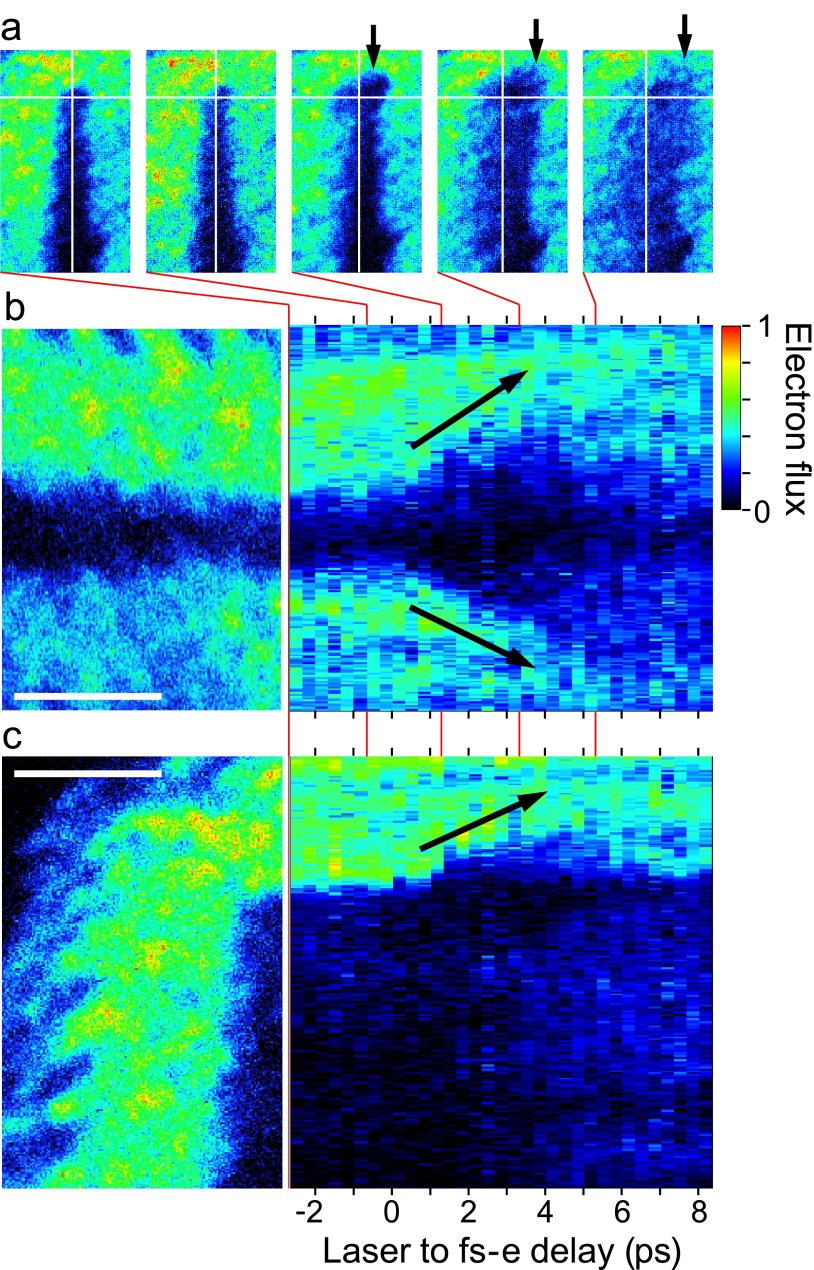
Femtosecond electron microscopy produces real-space images of matter in a series of ultrafast snapshots. Pulses of electrons self-disperse under space-charge broadening, so without compression, the ideal operation mode is a single electron per pulse. Here, we demonstrate femtosecond single-electron point projection microscopy (fs-ePPM) in a laser-pump fs-e-probe configuration. The electrons have an energy of only 150 eV and take tens of picoseconds to propagate to the object under study. Nonetheless, we achieve a temporal resolution with a standard deviation of 114 fs (equivalent to a full-width at half-maximum of 269 ± 40 fs) combined with a spatial resolution of 100 nm, applied to a localized region of charge at the apex of a nanoscale metal tip induced by 30 fs 800 nm laser pulses at 50 kHz. These observations demonstrate real-space imaging of reversible processes, such as tracking charge distributions, is feasible whilst maintaining femtosecond resolution. Our findings could find application as a characterization method, which, depending on geometry, could resolve tens of femtoseconds and tens of nanometres. Dynamically imaging electric and magnetic fields and charge distributions on sub-micron length scales opens new avenues of ultrafast dynamics. Furthermore, through the use of active compression, such pulses are an ideal seed for few-femtosecond to attosecond imaging applications which will access sub-optical cycle processes in nanoplasmonics.


Figures

FIG. 1.
FIG. 1.
(a) Schematic of the femtosecond electron point-projection microscope. A nanoscale metal tip (NSMT1) was illuminated with horizontally polarized λ = 800 nm, 30 fs laser pulses at a repetition rate of 50 kHz. The apex of NSMT1 had a radius of curvature of approximately 50 nm, and the laser pulses were transmission focused to a spot size of 5.4 μm. A pulse energy of 45 nJ produced a peak intensity of 1.2 × 1012 W cm−2, however, the apex of NSMT1 experienced less than 1/20th of this intensity. NSMT1 was held at a potential of −150 V with respect to a grounded TEM grid, accelerating the resultant femtosecond electron (fs-e) pulses towards a distant microchannel plate detector, forming a point-projection image. Nanoscale metal tip 2 (NSMT2) was illuminated by vertically polarized laser pulses from the same source and a comparable intensity. A significantly longer focusing optic (f = 300 mm as compared to f = 75 mm) illuminates a region above the apex of NSMT2, resulting in a localized time-varying charge distribution. (b) Low magnification to high magnification PPM images of NSMT2 using electrons emitted from NSMT1. Each image is the sum of 5 × 105 laser shots, and the colour scale is the normalized electron flux. From left to right, the scale bars are 250 μm, 50 μm, and 250 nm, and the corresponding maximum fluxes of 8 × 105, 4 × 105, and 2 × 104 electrons.
FIG. 2.
FIG. 2.
(a) Optical microscope image of a typical NSMT. (b) By thresholding and edge detection, a series of lines representing the typical shape of a NSMT is shown (black lines). The magenta line is the approximation to this shape used in the Superfish Poisson solver. (c) Superfish output of PPM geometry with the TEM grid at 0 V and the NSMT at −150 V. (d) Superfish field map at NSMT1, showing changing mesh size to accommodate millimetre flight length and nanometric tip apex. In (c) and (d), equipotentials are spaced by 10 V.
FIG. 3.
FIG. 3.
(a) Comparison of output of the GPT model (top) with experimental observations (bottom) of electron propagation from NSMT1, through a TEM grid at 2.45 mm from NSMT1, then on through a field free region to the detector 0.44 m distant. This agreement allows independent confirmation of magnification and source size. The scale bar is 350 μm at the TEM grid, and the colour scale is the normalized electron flux, where unity is equivalent to 105 electrons. (b) A direct comparison of the predicted and observed electron distribution following low magnification fs-ePPM. The agreement to the right of the dashed line is compromised by edge effects in the detector.
FIG. 4.
FIG. 4.
Femtosecond electron point-projection microscopy of nanoscale metal tip 2 (NSMT2) illuminated with an infrared 30 fs laser pulse. (a) Sequence of PPM images of NSMT2. Presented are (left to right) −2.66 ps, −0.67 ps, 1.33 ps, 3.33 ps, and 5.33 ps, where time zero is the point at which the fs-e and laser pulses arrive at NSMT2 simultaneously. Horizontal and vertical lines indicate positions of (b) and (c) which are time-dependent slices through the dataset, and the black arrows indicate the evolution of charging of NSMT2. (b) (Left) Part of the −2.67 ps spatial image below the white line, rotated clockwise by 90°. (Right) Sections through the time-dependent image dataset along the horizontal line in (a) as a function of laser-fs-e delay. Each slice is 9 pixels wide, corresponding to 50 nm. The flare indicated by the black arrows at positive delay is due to electron-electron scattering from apex of NSMT2 induced by strong-field electron ejection. (c) (Left) As (b) but for the left-hand part of the −2.67 ps image, followed by (right) the temporal evolution of 9 pixel wide slice as function of laser-fs-e delay. In all images, unity on the colour scale corresponds to 104 electrons summed over 5 × 105 laser shots, and the scale bars in (b) and (c) are 1 μm.
FIG. 5.
FIG. 5.
Comparison between the measured difference between large negative laser-fs-e pulse delay and subsequent fs-ePPM images (black squares), and the predicted cumulative electron flux at the plane of NSMT2 (coloured lines) as the average number of electrons per pulse is varied between zero electrons (No SC) and 10 electrons. The laser-induced charging of NSMT2 switches on rapidly but dissipates slowly, hence using the cumulative signal difference. The signal is found by taking a 9 × 9 square of pixels on subsequent images and taking the difference between the comparable points on the −2 ps dataset. The error bars are the result of combining the standard error of the mean of the 9 × 9 pixels at −2 ps with the equivalent SEM at subsequent delays in quadrature. The comparison of these measurements to the GPT predictions allows the number of electrons per pulse to be inferred.
FIG. 6.
FIG. 6.
Femtosecond electron pulse stretching on propagation from NSMT1 including space charge, geometric effects, and energy bandwidth. The solid lines are the predicted standard deviation of the fs-e pulse width as a function of time at different points along the flight path between NSMT1 and NSMT2. The SD duration of the space-charge free fs-e pulse increases along the flight path, a result of the geometric stretch and energy bandwidth. The contribution of space charge can also be observed as the average amount of total charge in the pulse is increased from no space charge (No SC) to 10 electrons per pulse. The dashed lines are the ±2σ width of the corresponding Gaussian distribution, i.e., 4 × SD. Experimental constraints are indicated by the grey regions. The vertical thin grey box indicates the position of NSMT2 with respect to NSMT1, and the horizontal grey boxes indicate an estimate of the rise time of the signal. The grey-level varies linearly with gradient of the signal, seen to be a maximum between 400 and 600 fs. The overlap between these regions and the dashed lines facilitates an estimate of the electron flux, which is most likely to be between less than one electron and two electrons per pulse.
FIG. 7.
FIG. 7.
Electron pulse spatial distribution as a function of arrival time at the plane of NSMT2 (colour density plots) and the corresponding histogram of the relative electron flux (magenta line). The total charge of the electron pulse is varied from (a) 0e (No SC), (b) 1e, (c) 2e, (d) 3e, (e) 5e, (f) 7e, and (g) 10e, with the total charge evenly distributed across the 50 000 GPT macro-particles used in the calculation. As the total charge of the pulse increases, a significant spatial and temporal spreading is found. The distribution best representing the results presented in Figure 5 are (a), (b), and (c).
FIG. 8.
FIG. 8.
Quantification of the number of laser shots required for real-space imaging with 800 nm, 30 fs laser illumination at 10 GW/cm2, and 150 eV electron pulses at one electron per pulse for a range of signal-to-noise ratios. The experimental results in Figure 5 correspond to an SNR of approximately 100 and were collected with 5 × 105 shots, indicated by the horizontal dashed line. The dimension of the unit cell of tungsten is 3.16 Å.

References

    1. Pellegrini C., Marinelli A., and Reiche S., “ The physics of x-ray free-electron lasers,” Rev. Mod. Phys. 88, 015006 (2016).10.1103/RevModPhys.88.015006 - DOI
    1. Tenboer J., Basu S., Zatsepin N., Pande K., Milathianaki D., Frank M., Hunter M., Boutet S., Williams G. J., Koglin J. E., Oberthuer D., Heymann M., Kupitz C., Conrad C., Coe J., Roy-Chowdhury S., Weierstall U., James D., Wang D., Grant T., Barty A., Yefanov O., Scales J., Gati C., Seuring C., Srajer V., Henning R., Schwander P., Fromme R., Ourmazd A., Moffat K., Van Thor J. J., Spence J. C. H., Fromme P., Chapman H. N., and Schmidt M., “ Time-resolved serial crystallography captures high-resolution intermediates of photoactive yellow protein,” Science 346, 1242–1246 (2014).10.1126/science.1259357 - DOI - PMC - PubMed
    1. Clark J. N., Beitra L., Xiong G., Higginbotham A., Fritz D. M., Lemke H. T., Zhu D., Chollet M., Williams G. J., Messerschmidt M., Abbey B., Harder R. J., Korsunsky A. M., Wark J. S., and Robinson I. K., “ Ultrafast three-dimensional imaging of lattice dynamics in individual gold nanocrystals,” Science 341, 56–59 (2013).10.1126/science.1236034 - DOI - PubMed
    1. Moore R. G., Lee W. S., Kirchman P. S., Chuang Y. D., Kemper A. F., Trigo M., Patthey L., Lu D. H., Krupin O., Yi M., Reis D. A., Doering D., Denes P., Schlotter W. F., Turner J. J., Hays G., Hering P., Benson T., Chu J.-H., Devereaux T. P., Fisher I. R., Hussain Z., and Shen Z.-X., “ Ultrafast resonant soft x-ray diffraction dynamics of the charge density wave in tbte3,” Phys. Rev. B 93, 024304 (2016).10.1103/PhysRevB.93.024304 - DOI
    1. Ruska E., “ The development of the electron microscope and of electron microscopy,” in Nobel Lecture, 1986. - PubMed