Fast electronic resistance switching involving hidden charge density wave states
- PMID: 27181483
- PMCID: PMC4873615
- DOI: 10.1038/ncomms11442
Fast electronic resistance switching involving hidden charge density wave states
Abstract
The functionality of computer memory elements is currently based on multi-stability, driven either by locally manipulating the density of electrons in transistors or by switching magnetic or ferroelectric order. Another possibility is switching between metallic and insulating phases by the motion of ions, but their speed is limited by slow nucleation and inhomogeneous percolative growth. Here we demonstrate fast resistance switching in a charge density wave system caused by pulsed current injection. As a charge pulse travels through the material, it converts a commensurately ordered polaronic Mott insulating state in 1T-TaS2 to a metastable electronic state with textured domain walls, accompanied with a conversion of polarons to band states, and concurrent rapid switching from an insulator to a metal. The large resistance change, high switching speed (30 ps) and ultralow energy per bit opens the way to new concepts in non-volatile memory devices manipulating all-electronic states.
Figures

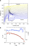
 is determined by τRC=RC where R is the two-terminal circuit resistance and changes from 53 to 44 ns. Fits of the relaxation times show that the difference between τ after switching and τRC at the end of the pulse is<0.3 ns, setting a limit on the intrinsic speed of the device. The insert shows the measuring circuit. The small superimposed oscillations are due to ringing of the circuit. Scale bar, 2 μm.


References
-
- Ichikawa H. et al.. Transient photoinduced ‘hidden' phase in a manganite. Nat. Mater. 10, 101–105 (2011). - PubMed
-
- Stojchevska L. et al.. Ultrafast switching to a stable hidden quantum state in an electronic crystal. Science 344, 177–180 (2014). - PubMed
-
- Nasu K. Photoinduced Phase Transitions World Scientific Publishing Company Incorporated (2004).
-
- Tokura Y. Photoinduced phase transition: a tool for generating a hidden state of matter. J. Phys. Soc. Jpn 75, 011001 (2006).
Publication types
Grants and funding
LinkOut - more resources
Full Text Sources
Other Literature Sources
Research Materials

