. 2016 May 16:6:25757.
doi: 10.1038/srep25757.

Geometric conductive filament confinement by nanotips for resistive switching of HfO2-RRAM devices with high performance

Affiliations

Geometric conductive filament confinement by nanotips for resistive switching of HfO2-RRAM devices with high performance

Gang Niu et al. Sci Rep. .

Abstract

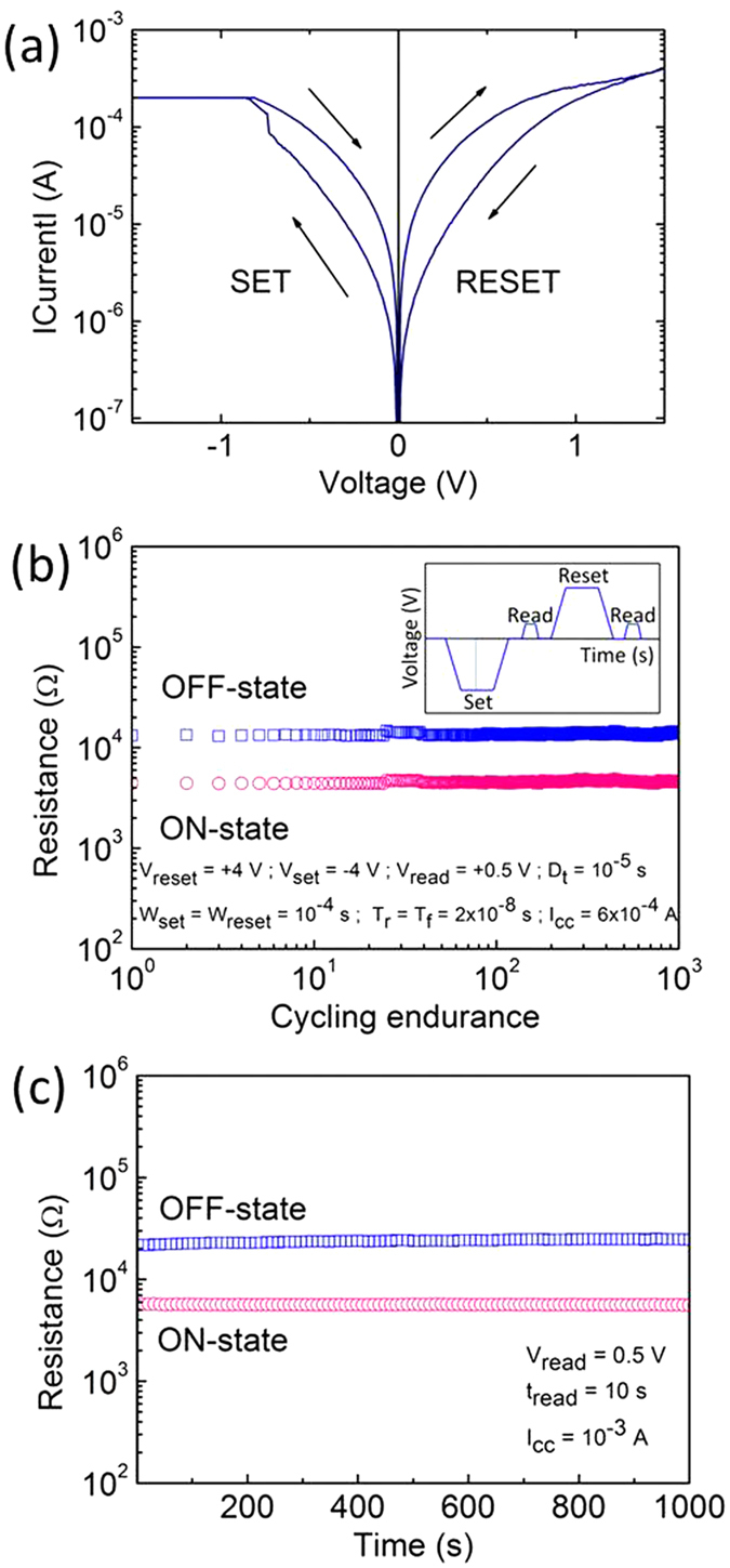
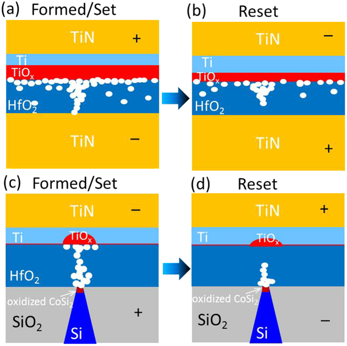
Filament-type HfO2-based RRAM has been considered as one of the most promising candidates for future non-volatile memories. Further improvement of the stability, particularly at the "OFF" state, of such devices is mainly hindered by resistance variation induced by the uncontrolled oxygen vacancies distribution and filament growth in HfO2 films. We report highly stable endurance of TiN/Ti/HfO2/Si-tip RRAM devices using a CMOS compatible nanotip method. Simulations indicate that the nanotip bottom electrode provides a local confinement for the electrical field and ionic current density; thus a nano-confinement for the oxygen vacancy distribution and nano-filament location is created by this approach. Conductive atomic force microscopy measurements confirm that the filaments form only on the nanotip region. Resistance switching by using pulses shows highly stable endurance for both ON and OFF modes, thanks to the geometric confinement of the conductive path and filament only above the nanotip. This nano-engineering approach opens a new pathway to realize forming-free RRAM devices with improved stability and reliability.


Figures

Figure 1
Figure 1. STEM-EDX performed on the cross-section of a TiN/Ti/HfO2/CoSi2/Si tip device.
(a) STEM image overview showing three Si tips; (b) High magnification STEM image on the squared device part in (a). (c) EDX chemical analysis of the same region in (b) and the element of Si, O, Co, N, Ti and Hf are represented by the color of black, white, blue, pink, orange and green, respectively. The arrows in (c) mark the partly oxidized Ti and CoSi2 layer.
Figure 2
Figure 2
FEM calculated maps of Ti/HfO2/CoSi2/Si-tip heterostructure on a 2D slice in 3D cylinder coordinates of (a) the electrical field distribution and (b) the ionic current density (VO) distribution. (c) Evolution of the electric field |E| in the ~10 nm HfO2 film at the sites 1 nm above the center (blue triangles) and above the edge (red squares) as a function of the tip radius.
Figure 3
Figure 3. AFM measurements performed on the HfO2 surface without top electrodes.
(a) Topography. (b,c) Current maps (TUNA) with bias of −8 V and −10 V, respectively. The black spots marked by red circles in (c) are conductive spots (the end of CFs) on the nanotip locations.
Figure 4
Figure 4. Electrical characterization of the TiN/Ti/HfO2/CoSi2/Si-tips device.
(a) Typical DC sweeps showing the evolution of the current intensity as a function of the voltage. (b) Pulse cycling endurance showing the evolution of the OFF- and ON-resistance states as a function of the number of cycles. The experimental details are shown in the inset and remarks in the figure. (c) Retention measurement performed at room temperature with experimental details shown in the figure remarks.
Figure 5
Figure 5
Schematic illustration of the VO (white circles) distribution of planar electrode MIM devices in (a) the Formed/Set state and (b) the Reset state, in which the VO distribution as well as the filament is not confined thus leading to instable endurance; (c) the filament formation of Si-tip electrode MIM devices in the Formed/Set state, in which the VO distribution and the filament is geometrically confined around the tip area; (d) the filament rupture during Reset process.

References

    1. Zhang K. Embedded Memories for Nano-Scale VLSIs (Springer, 2009).
    1. Yu S. et al.. A Low Energy Oxide-Based Electronic Synaptic Device for Neuromorphic Visual Systems with Tolerance to Device Variation. Adv. Mater. 25, 1774–1779 (2013). - PubMed
    1. Waser R. Nanoelectronics and Information Technology 3rd edn, 692 (Wiley-VCH, 2012).
    1. Jousseaume V. et al.. Comparative Study of Non-Polar Switching Behaviors of NiO- and HfO2-based Oxide Resistive-RAMs. Solid-State Electron 58, 62–67 (2011).
    1. Chiu F.-C., Li P.-W. & Chang W.-Y. Reliability Characteristics and Conduction Mechanisms in Resistive Switching Memory Devices using ZnO Thin Films. Nanoscale Res. Lett. 7, 178 (2012). - PMC - PubMed

Publication types