. 2016 May 20:7:11566.
doi: 10.1038/ncomms11566.

Multifunctional hydrogel nano-probes for atomic force microscopy

Affiliations

Multifunctional hydrogel nano-probes for atomic force microscopy

Jae Seol Lee et al. Nat Commun. .

Abstract

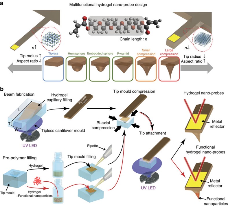
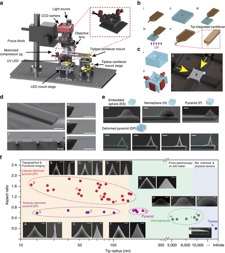
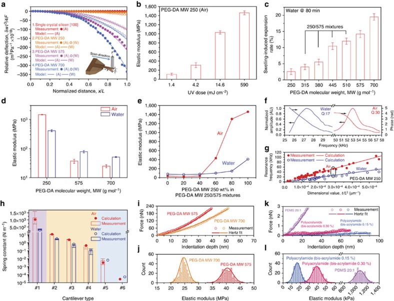
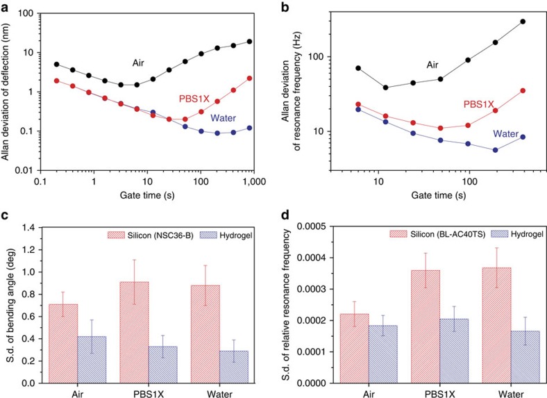
Since the invention of the atomic force microscope (AFM) three decades ago, there have been numerous advances in its measurement capabilities. Curiously, throughout these developments, the fundamental nature of the force-sensing probe-the key actuating element-has remained largely unchanged. It is produced by long-established microfabrication etching strategies and typically composed of silicon-based materials. Here, we report a new class of photopolymerizable hydrogel nano-probes that are produced by bottom-up fabrication with compressible replica moulding. The hydrogel probes demonstrate excellent capabilities for AFM imaging and force measurement applications while enabling programmable, multifunctional capabilities based on compositionally adjustable mechanical properties and facile encapsulation of various nanomaterials. Taken together, the simple, fast and affordable manufacturing route and multifunctional capabilities of hydrogel AFM nano-probes highlight the potential of soft matter mechanical transducers in nanotechnology applications. The fabrication scheme can also be readily utilized to prepare hydrogel cantilevers, including in parallel arrays, for nanomechanical sensor devices.


Figures

Figure 1
Figure 1. Design and fabrication of hydrogel AFM nano-probes.
(a) Conceptual schematic for beam and tip geometry to tune probe characteristics for various AFM applications. Capillary driven filling of ultraviolet curable hydrogels into the engineered beam mould facilitates fabrication of tipless hydrogel cantilevers with tunable spring constants over several orders of magnitude by varying the MW of the monomer composition and geometrical dimensions of the cantilever. Nanoscale dimensions of the tip shape can also be tuned by preparing different tip moulds or by applying deformation to a given mould. When the tip mould is compressed, the tip becomes sharper and the tip aspect ratio typically increases. (b) Fabrication method for hydrogel AFM probes. A tipless hydrogel cantilever is first prepared by ultraviolet curing of the pre-polymer solution introduced into the cantilever beam mould. The tipless hydrogel cantilever then makes contact with a tip mould filled with pre-polymer solution without or with encapsulated functional elements, followed by a second round of ultraviolet exposure which cures the hydrogel in the tip mould and results in firm attachment between the cantilever and tip. Before the second ultraviolet exposure, the hydrogel-filled tip mould can be optionally deformed by applying bi-axial compressive strains to facilitate tunable tip sharpness and aspect ratio.
Figure 2
Figure 2. Replica moudling strategy to fabricate hydrogel nano-probes.
(a) Experimental set-up for fabricating hydrogel nano-probes, which consists of a custom-built microscope, a ultraviolet light-emitting diode (LED), and a compression jig for tip shape tuning. (b) Tip integration process (i) Fabricated tipless hydrogel cantilever, (ii) Fill the pre-polymer solution into a tip mould (in this case, an inverted pyramid although the design can vary), (iii) Approach the tipless hydrogel cantilever towards the hydrogel-filled tip mould and make contact between the cantilever and tip mould, (iv) Cure hydrogel tip with ultraviolet light, (v) Separate the tip-integrated hydrogel cantilever from tip mould). (c) Tip shape tuning via compression replica moudling (i) PDMS pyramidal tip mould, (ii) bi-axial compression to the tip mould and 3D schematic (iii) for bi-axial compression of the tip mould. (d) Scanning electron and optical micrographs of a single tipless hydrogel cantilever (i) and its array (ii). Tipless hydrogel cantilevers with lengths of (iii) 300, (iv) 500 and (v) 700 μm, respectively. Scale bars are 20, 200 and 500 μm, for (i), (ii) and (iii–v), respectively. (e) Scanning electron micrographs showing different tips integrated on hydrogel cantilevers—embedded sphere (ES), hemisphere (H), pyramid (P) and deformed pyramid (DP). All scale bars are 10 μm. (f) Summary of tip radii and aspect ratios of various deformed pyramidal tips. Scale bars are 5 μm for overall views, 200 nm for the zoom-ins of A and B, and 1 μm for the other zoom-ins (C–G).
Figure 3
Figure 3. Tunable mechanical properties of hydrogel nano-probes for force-sensing applications.
(a) Relative deflection of hydrogel cantilevers as a function of normalized displacement. ‘A' and ‘W' represent air and water, respectively. (b) Elastic moduli of PEG-DA MW 250 hydrogel cured under different ultraviolet doses. Error bars represent s.d. of the mean with N=3 measurements. (c) Swelling-induced expansion of PEG-DA hydrogels in water. (d) Elastic moduli of PEG-DA MW 250, 575 and 700 in air and water. Error bars represent s.d. of the mean with N=3 measurements. (e) Elastic moduli of PEG-DA MW 250/575 mixtures in air and water as a function of wt% of PEG-DA MW 250. (f) Resonance spectra of a hydrogel cantilever in air and water (length, width and thickness: 222, 50 and 15 μm). (g) Resonance frequencies of various hydrogel cantilevers with different dimensions in air and water. The two data points enclosed by the ellipse correspond to the measurement values for the hydrogel cantilever shown in f. A total of 53 and 35 measurements were completed in air and water, respectively. (h) Experimental and theoretical spring constant values for hydrogel cantilevers in air and water (length, width and thickness: 500, 350 and 100 μm (#1); 220, 50 and 19 μm (#2); 400, 50 and 20 μm (#3); 375, 50 and 11 μm (#4); 505, 50 and 11 μm (#5); and 1500, 35 and 5 μm (#6)). Cantilevers #1–4 were fabricated using PEG-DA MW 250, and cantilevers #5 and #6 were fabricated using PEG-DA MW 700. Error bars represent s.d. of the mean with N=3 measurements. (i) Force-indentation curves on PEG-DA hydrogel slabs in air with Hertzian curve fits. (j) Elastic moduli of different MW PEG-DA samples in air. (k) Force-indentation curves on different polymeric substrates in water with Hertzian curve fits. (l) Elastic moduli of PDMS 20:1 and polyacrylamide with different bis-acrylamide concentrations in water.
Figure 4
Figure 4. Stability of hydrogel probes in different environmental conditions.
(a,b) Allan deviation of the static deflection of a hydrogel probe (length, width and thickness: 240, 50 and 10 μm) (a) and Allan deviation of the resonance frequency of another hydrogel probe (length, width and thickness: 220, 50 and 20 μm) (b) in air, water and PBS solution. (c,d) S.d. of the bending angles of three silicon (NSC36-B, Mikromasch) and three hydrogel probes with similar spring constants (c) and s.d. of the relative resonance frequencies of three silicon (BL-AC40TS, Olympus) and three hydrogel probes with similar resonance frequencies in air, water and PBS solution. Error bars represent s.d. of the average from three measurements for each device (N=9 measurements for each probe material).
Figure 5
Figure 5. Noncontact mode imaging performance of hydrogel probes and comparison with silicon probes.
(a) Noncontact mode height images of calibration gratings (silicon and PDMS replica), digital versatile disk media with written data bits, nanowires, aluminium foil, graphitic layers, nanodisks and an AAO sample (70 nm pore diameter). Scale bars are 5, 5, 5, 10, 1, 5, 0.4 and 0.1 μm for (i–viii), respectively. (b) Top (i) and side (ii) view of SEM images of cylindrical pores with 1 μm diameter, 1.4 μm pitch and 5 μm depth. The side view was taken after the sample was cleaved. Scale bars are 1 μm. (c) Scanning electron microscopy (SEM) images showing tip apex regions of commercial silicon (PPP-NCHR, Nanosensors) and fabricated hydrogel (length, width and thickness: 200, 50 and 20 μm) probes and corresponding 3D representations of noncontact height images for the deep cylindrical pores. All scale bars are 1 μm. (d) Local aspect ratio (i) and maximum depth (ii) measured with silicon and hydrogel probes. (e) Height images for another AAO sample (35 nm pore diameter) taken by commercial silicon (PPP-NCHR, Nanosensors) and fabricated hydrogel (length, width and thickness: 170, 50 and 20 μm) probes at 1, 5, 10, 25, 50 and 1 Hz, respectively. Height images are 2D fast Fourier transformed (2D FFT) to quantitatively compare image distortions and artifacts. Scale bars for height and 2D FFT images are 100 nm and 200 μm−1, respectively. The same colour bars are used for height and 2D FFT images, respectively.
Figure 6
Figure 6. Contact mode imaging results in liquid using hydrogel probes and performance comparison with silicon probes.
(a) Contact mode height images, with fixed 3 nN contact forces, for human fibroblast cells (MRC-5) in PBS imaged by a commercial silicon probe (first row) and a fabricated hydrogel probe (second row) at various scan rates. All scale bars are 5 μm. (b) Height profiles along the A–A′ and B–B′ lines in a. (c) Contact mode height images, with fixed 300 nN contact force, for MRC-5 cells in PBS sequentially imaged by using hydrogel (first), silicon (second) and hydrogel (third) probes at a scan rate of 1 Hz. All scale bars are 5 μm. (d) Height profiles along the A–A′ line in c.
Figure 7
Figure 7. Wear characteristics of hydrogel nano-probes and regeneration via oxygen plasma ashing.
(a) Scanning electron microscopy (SEM) images of hydrogel probe tips taken before and after wear tests. Imaging mode, condition and surrounding media are indicated on the left side of each micrograph. A hard silicon calibration grating sample was used for test cases 1–4, and a PDMS calibration grating sample replicated from the silicon grating was used for test case 5. All scale bars are 500 nm. (b) Increased tip radius and total wear volume after scanning a 0.246-m length (12 frame imagings with a scan size of 40 × 40 μm2) for each operating condition. (c) SEM images of worn hydrogel nano-probe tips before (i, ii) and after (iii, iv) oxygen plasma ashing. Hydrogel nano-probes with tip radii of 130 and 340 nm were re-sharpened to have sub 30 nm tip radii after plasma ashing. All scale bars are 5 μm.
Figure 8
Figure 8. Programming of multifunctional hydrogel nano-probes.
(a) Hydrogel nano-probes with integrated functional nanomaterials achieved through materials encapsulation. Depending on the encapsulated nanomaterial, the tip structure is composed of PEG-DA with varying MW as specified: (i, ii) Rhodamine B dye (MW 575), (iii, iv) cadmium telluride (CdTe) quantum dots (MW 700), (v, vi) cobalt (Co) nanoparticles (MW 250) and (vii, viii) gold (Au) nanoparticles (MW 700). The mesh sizes of PEG-DA monomers with different MWs are presented. All scale bars are 10 μm. (b) Multifunctional hydrogel nano-probes with sequential loading of FITC and Rhodamine B (i), CdTe quantum dots and Co nanoparticles (ii), and CdTe quantum dots and gold nanoparticles (iii). All scale bars are 10 μm. (c) Schematic for local inductive heating. (d) Normalized amplitude spectra of a hydrogel nano-probe with a Co nanoparticle-embedded tip under induction heating in water. (e) Resonance frequency shift as a function of the input power. (f) Schematic for local temperature sensing via fluorescence quenching of quantum dots. (g) Fluorescence spectra from a hydrogel nano-probe with a CdTe quantum dot-embedded tip in contact with an ITO-coated glass substrate under Joule heating in water. (h) Peak wavelength shift and the normalized peak intensity as a function of the temperature at the tip contact point. (i) Schematic for a dual function hydrogel nano-probe for local heating and temperature sensing. (j) Fluorescence spectra from a hydrogel nano-probe with sequentially embedded CdTe quantum dots and Co nanoparticles under induction heating. (k) Temperature increase as a function of the power applied to the induction coil. (l) Schematic for localized materials delivery. (m) Bright-field and fluorescence microscopy images of a hydrogel nano-probe before (i) and after (ii) the first loading as well as after the first delivery (iii) and after the second loading (iv), respectively. All scale bars are 20 μm. (n) Bright-field optical microscopy image (i) and fluorescence microscopy image (ii) for a breast cancer cell (MCF-7) demonstrating localized delivery of Rhodamine B dye. Scale bars are 10 μm. All error bars represent the s.d. of the mean with N=3 measurements.

Similar articles

Cited by

References

    1. Bottomley L. A. Scanning probe microscopy. Anal. Chem. 70, 425–476 (1998). - PubMed
    1. Binnig G. & Rohrer H. Scanning tunneling microscopy. IBM J. Res. Dev. 44, 279–293 (2000).
    1. Binnig G., Quate C. F. & Gerber C. Atomic force microscope. Phys. Rev. Lett. 56, 930–933 (1986). - PubMed
    1. Bull M. S., Sullan R. M. A., Li H. & Perkins T. T. Improved single molecule force spectroscopy using micromachined cantilevers. ACS Nano 8, 4984–4995 (2014). - PubMed
    1. Li M., Tang H. X. & Roukes M. L. Ultra-sensitive NEMS-based cantilevers for sensing, scanned probe and very high-frequency applications. Nat. Nanotechnol. 2, 114–120 (2007). - PubMed

Publication types