

doi: 10.1039/C3BM60280J.
Epub 2014 Jan 9.
Nanoscale Semiconductor Devices as New Biomaterials
Affiliations
- PMID: 27213041
- PMCID: PMC4874554
- DOI: 10.1039/C3BM60280J
Item in Clipboard
Nanoscale Semiconductor Devices as New Biomaterials
Biomater Sci.
.
Abstract
Research on nanoscale semiconductor devices will elicit a novel understanding of biological systems. First, we discuss why it is necessary to build interfaces between cells and semiconductor nanoelectronics. Second, we describe some recent molecular biophysics studies with nanowire field effect transistor sensors. Third, we present the use of nanowire transistors as electrical recording devices that can be integrated into synthetic tissues and targeted intra- or extracellularly to study single cells. Lastly, we discuss future directions and challenges in further developing this area of research, which will advance biology and medicine.
Figures
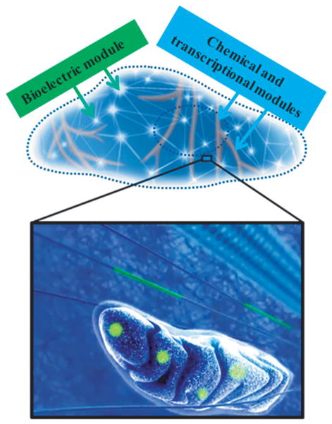
The top panel depicts how bioelectric, and chemical and transcriptional modules form networks inside cells. Shown in the lower panel are single mitochondrion and microtubule bundles containing these modules, both of which can be used as intracellular electrical interfaces with nanoscale semiconductor devices shown in green.
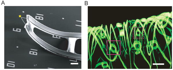
(A) Scanning electron microscopy image of a single kinked nanowire probe used for intracellular potential recording. The yellow star highlights the position of a field effect transistor. Scale bar, 5 μm. (B) Confocal fluorescence microscopy image of a macroporous nanoelectronic scaffold used for sensing from engineered tissues. Magenta boxes demarcate two field effect transistor devices. Scale bar, 20 μm.
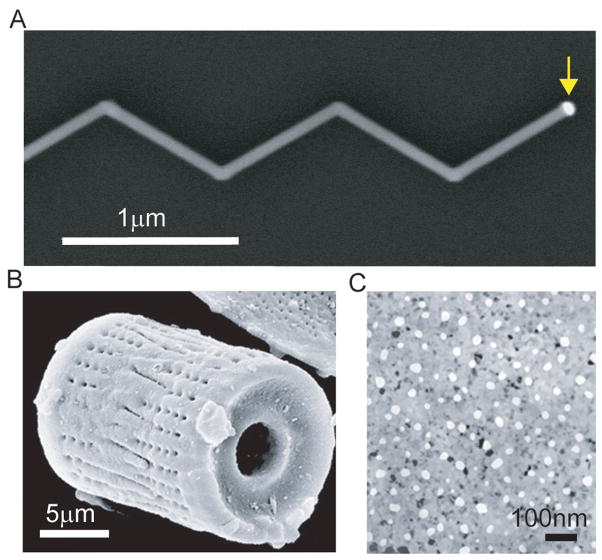
(A) Scanning electron microscopy image of a kinked nanowire; yellow arrow highlights the gold catalyst used for VLS growth. (B) A silicon ‘diatom’ synthesized by magnesium reduction. (C) A nanoporous silicon membrane used for molecular separation. B and C are adapted from Reference and , respectively, with the permission from Nature Publishing Group.
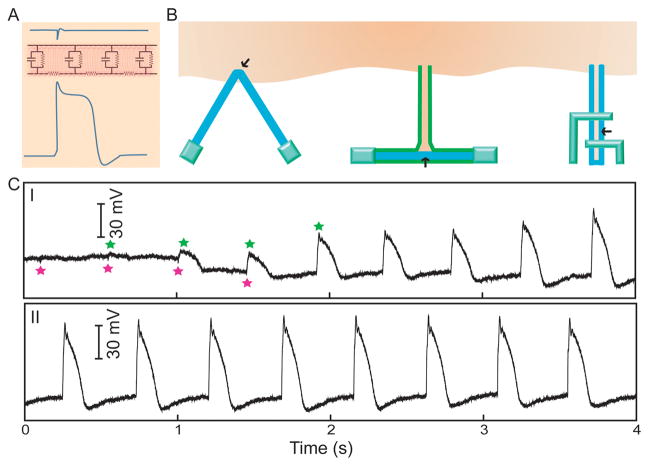
(A) Plot comparing the amplitude of intracellular (lower) vs extracellular (upper) FET recordings, with shape ‘distortions’ due to the resistor-capacitor (RC) components from plasma membrane (middle). (B) Several FET configurations for intracellular recording. The black arrows indicate the sensing domains. (C) Electrical recording traces from a kinked nanowire probe as it transitions (I) from an extracellular (magenta stars) to intracellular (green stars) space, and (II) reaches an intracellular steady state.
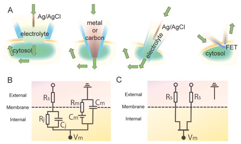
(A) Four intracellular recordings are depicted: glass micropipette, metal or carbon micro/nanoelectrode, glass micropipette, and nanoFET (from left to right). The green arrows indicate the current flows. (B) and (C) are the equivalent circuits of the intracellular junctions established through conventional devices and nanoFET, respectively. Abbreviations: Cj, junction capacitance; Cm, membrane capacitance; Rs, series resistance; Rj, junction resistance; Rm, membrane resistance; Vm, intracellular potential.
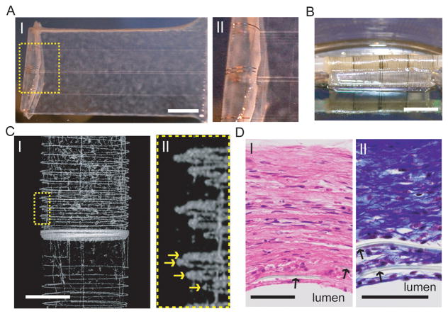
(A) (I) Photograph of a single HASMC sheet cultured with sodium L-ascorbate on a nanoES. (II) Zoomed-in view of the dashed area in (I), showing metallic interconnects macroscopically integrated with cellular sheet. (B) Photograph of the vascular construct after rolling into a tube and maturation in a culture chamber for 3 weeks. (C) (I) Micro-computed tomograph of a tubular construct segment. (II) Zoomed-in view of (I). Yellow arrows mark the individual nanowire FET-containing layers of the rolled construct. Scale bar, 1 mm. (D) (I) Hematoxylin & eosin and (II) Masson Trichrome (;collagen is blue) stained sections of nanoelectronic-HASMC hybrid (~ 6 μm thick) cut perpendicular to the tube axis; lumen regions are labeled. Black arrows mark the positions of SU-8 ribbons of the nanoES. Scale bars, 50 μm.
References
Grants and funding
LinkOut - more resources
Full Text Sources
Other Literature Sources