

Review
doi: 10.1038/ncomms11495.
Quantum mechanical effects in plasmonic structures with subnanometre gaps
Affiliations
- PMID: 27255556
- PMCID: PMC4895716
- DOI: 10.1038/ncomms11495
Item in Clipboard
Review
Quantum mechanical effects in plasmonic structures with subnanometre gaps
Nat Commun.
.
Abstract
Metallic structures with nanogap features have proven highly effective as building blocks for plasmonic systems, as they can provide a wide tuning range of operating frequencies and large near-field enhancements. Recent work has shown that quantum mechanical effects such as electron tunnelling and nonlocal screening become important as the gap distances approach the subnanometre length-scale. Such quantum effects challenge the classical picture of nanogap plasmons and have stimulated a number of theoretical and experimental studies. This review outlines the findings of many groups into quantum mechanical effects in nanogap plasmons, and discusses outstanding challenges and future directions.
Figures
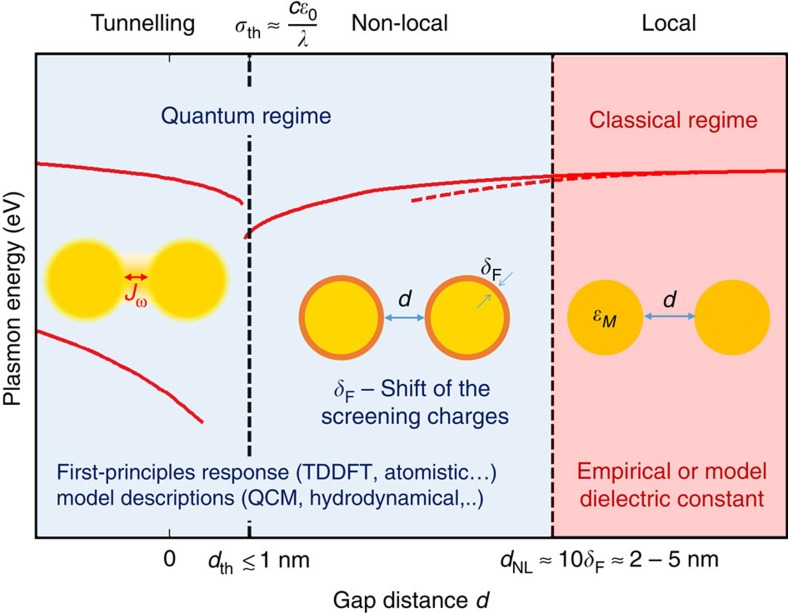
Sketch of the different regimes for the plasmon resonances of a sphere-dimer in vacuum identified as a function of the gap distance d. These regimes are illustrated by the energies of the plasmonic modes predicted by the classical (red dashed line) and quantum calculations (solid lines). For large gap distances, the system is in the classical regime and its response can be described using Maxwell's equations with empirical or model local dielectric constants of the metal ɛM. In the nonlocal regime (d<dNL), the actual position of the screening charges with respect to the geometrical boundaries given by δF leads to an effective correction of the ‘physical' gap distance compared with the geometrical gap distance d. The nonlocal screening leads to deviations between the classical (dashed line) and quantum descriptions (solid line). In the tunnelling regime, the ac tunnelling current Jω across the junction strongly changes the optical response, when the conductivity of the junction becomes larger than σth (which sets the corresponding threshold gap distance dth). The plasmon modes of the separated dimer are progressively extinguished, and the CTP modes emerge before their direct geometrical overlap. We denote the distance range where the electric tunnelling and/or the nonlocal screening are important as the ‘quantum regime'. The plasmonic resonance in this regime can be addressed using ab-initio approaches or model descriptions. The transition between the different regimes is smooth and the boundaries shown in the figure are only indicative.
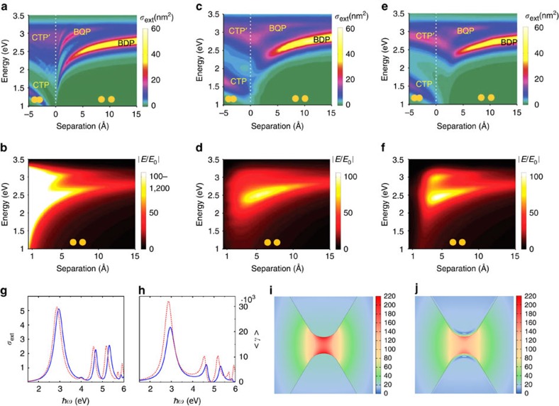
(a–f) Comparison of the optical properties of a metallic dimer simulated with (a,b) local Drude model, (c,d) TDDFT calculation and (e,f) the QCM. The dimer consists of two Na spheres with radii of 2.17 nm. (a,c,e) The colour plots of the extinction spectra σext as a function of gap distances. (b,d,f) The simulated near-field enhancements as a function of gap distances. The relevant plasmon modes are labelled: bonding dimer plasmon (BDP), bonding quadrupolar plasmon (BQP), charge transfer plasmon (CTP) and higher-order charge transfer plasmon (CTP'). (a–f) Images are reproduced from ref. . Copyright 2014 Nature Publishing Group. (g–j) Simulations of nonlocal effects for a metallic bowtie dimer. The dimer consists of two Au wires with cross-sections comprising equilateral triangles (side length: 45 nm, gap distance: 1 nm, tip radius of curvature: 1 nm). (g) Extinction cross-section spectra σext and (h) the near-field enhancement <γ> calculated from the local classical model (red dashed lines) and the NLHD model (blue solid lines). (i,j) Near-field distribution around the gap region of the Au bow-tie dimer calculated from (i) the local classical model and (j) the NLHD model. The colour scales in i,j represent the enhancement of the electric near-field. (g–j) Figures adapted with permission from ref. .
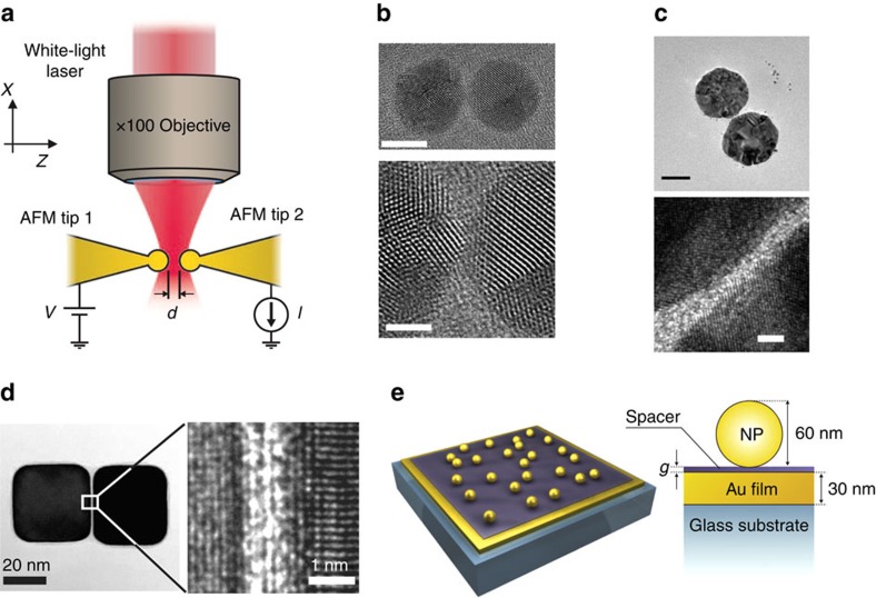
(a) Schematic illustration of the plasmonic dimer formed by pushing two AFM cantilevers in tip-to-tip configuration. Reproduced from ref. . Copyright 2012 Nature Publishing Group. (b) High-resolution TEM images of Ag nanosphere dimer formed by pushing two Ag nanoparticles together using focused electron beam. The diameter of each Ag nanoparticle is 9 nm. Top panel: overview of the dimer. Scale bar is 5 nm. Bottom panel: Zoomed-in view of the Ag dimer showing the gap distance d≈3.5 Å. Scale bar is 2 nm. Reprinted with permission from ref. . Copyright 2013 American Chemical Society. (c) TEM image of Au nanodisk dimer form by two-step electron beam lithography. The diameter of each nanodisk is 90 nm. Top panel: overview of the dimer. Scale bar is 50 nm. Bottom panel: zoomed-in view of the Au dimer showing the gap distance d≈2.0 Å. Scale bar is 2 nm. Reproduced from ref. . Copyright 2014 Nature Publishing Group. (d) High-resolution TEM image of the Ag dimer formed by linking molecules, with zoomed-in TEM image showing the subnanometre gap distance. Image reproduced from ref. . Copyright 2014 AAAS. (e) Schematic of particle-on-film geometry, with the nanoscale gap defined by a thin self-assembled monolayer layer. Image reproduced from ref. . Copyright 2012 AAAS.
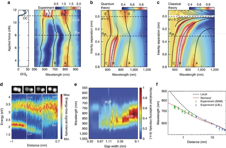
(a) Simultaneously measured electrical conductance (G/G0) and dark-field scattering of the AFM dimer shown in Fig. 3a with increasing force applied to the inter-tip cavity after snap-to-contact. The bonding plasmon modes are labelled as A, B and C. The CTP modes are labelled as D and E. (b) QCM and (c) local classical model simulations of the tip-based dimer. The colour scales in a–c represent relative scattering intensities. (a–c) Reproduced from ref. . Copyright 2012 Nature Publishing Group. (d) EELS spectra of the Ag dimers shown in Fig. 3b as the gap distance changes from 7 Å to –1 nm. STEM images (top panels) collected at the beginning and end of each scan (highlighted by white solid vertical lines) indicate the gap distances of +7 Å,<2.7 Å, −3 Å and −1 nm from right to left. Reprinted with permission from ref. . Copyright 2013 American Chemical Society. (e) Dark-field scattering spectra of the EBL-fabricated Au nanodisk dimers shown in Fig. 3c with various gap distances. Reproduced from ref. . Copyright 2014 Nature Publishing Group. (f) Peak wavelengths (green circles and blue diamonds) of the dark-field scattering spectra of the particle-on-film structure shown in Fig. 3e as a function of gap distance. Wavelengths deviate from expectations of local classical simulations (black dashed line) at small gap distances, but can be explained with nonlocal models (solid red line). Error bars represent the uncertainty in determining the wavelength of the plasmon resonance peak. Image reproduced from ref. . Copyright 2012 AAAS.
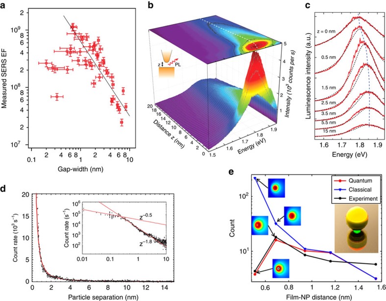
(a) SERS enhancement factors measured for Au dimers shown in Fig. 3c with various gap distances. Largest enhancement is obtained for dimer with gap distance ≈6.7 Å. The horizontal error bars represent the uncertainties in retrieving the gap-width from TEM images. The vertical error bars originate from the uncertainties in the reference Raman measurements. Reproduced from ref. . Copyright 2014 Nature Publishing Group. (b) Gap distance dependence of photoluminescence intensity in STM-based measurements (experimental configuration schematically illustrated in inset). (c) Corresponding PL spectra for different gap distances in these STM-based measurements. (b,c) Images are reprinted with permission from ref. . Copyright 2014 American Chemical Society. (d) Four-wave mixing photon count rate as a function of gap between two 60-nm-diameter gold nanoparticles. The inset shows a detailed view on a log–log scale. Reprinted with permission from ref. . Copyright 2007 American Physical Society. (e) Third harmonic generation as a function of SAM thickness in particle-on-film geometry (inset), comparing the measurements (black line) with the classical (blue line) and QCM (red line) calculations. Insets show near-field distributions simulated using QCM and local Drude models. Reprinted with permission from ref. . Copyright 2014 American Chemical Society.
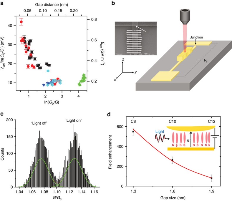
(a) Optical rectification voltage Vopt as a function of gap distance (top axis) or junction conductance G (bottom axis) for nanogap junctions fabricated via electromigration. Error bars indicate the statistical uncertainty in Vopt and ln G. Image reproduced from ref. . Copyright 2010 Nature Publishing Group. (b) Schematic illustration of an Au electrical plasmon detector. Creation of SPPs is achieved by normal illumination of the grating by a laser via a microscope objective. (c) SPP-modulated conductance histogram measured with the set-up in b. Irradiation appears to shift the Gaussian describing the distribution of conductance values around ∼1G0 (‘light-off' conductance) to a new and higher mean value (‘light-on' conductance). (b,c) Images are reprinted with permission from ref. . Copyright 2011 American Chemical Society. (d) Field enhancement in a plasmonic nanogap estimated from the rectification current. Reprinted with permission from ref. . Copyright 2011 American Chemical Society.
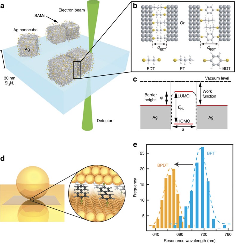
(a) Schematic illustration of a molecular junction made of two Ag nanoparticles linked by a SAM layer. (b) The distance between the two nanoparticles is determined by the thickness of the SAMs. (c) A charge transfer channel between the Ag nanoparticles can be opened by lowering the tunnelling barrier using molecules. (a–c) Images reproduced from ref. . Copyright 2014 AAAS. (d) Schematic illustration of the molecular junction formed in particle-on-film geometry. (e) Plasmon resonance wavelengths can be tuned by controlling the concentration of the two types of molecules (biphenyl-4-thiol (BPT) and biphenyl-4,4'-dithiol (BPDT)). (d,e) Images are reprinted with permission from ref. . Copyright 2015 American Chemical Society.
References
-
- Maier S. A. Plasmonics: Fundamentals and Applications Springer (2007).
-
- Halas N. J. Plasmonics: an emerging field fostered by Nano Letters. Nano Lett. 10, 3816–3822 (2010). - PubMed
-
- Hao E. & Schatz G. C. Electromagnetic fields around silver nanoparticles and dimers. J. Chem. Phys. 120, 357–366 (2004). - PubMed
-
- Crozier K. B., Sundaramurthy A., Kino G. S. & Quate C. F. Optical antennas: Resonators for local field enhancement. J. Appl. Phys. 94, 4632–4642 (2003).
-
- Yu N. et al.. Light propagation with phase discontinuities: generalized laws of reflection and refraction. Science 334, 333–337 (2011). - PubMed
Publication types
LinkOut - more resources
Full Text Sources
Other Literature Sources
Miscellaneous
