

Efficient plasmonic emission by the quantum Čerenkov effect from hot carriers in graphene
- PMID: 27293014
- PMCID: PMC4910017
- DOI: 10.1038/ncomms11880
Efficient plasmonic emission by the quantum Čerenkov effect from hot carriers in graphene
Abstract
Graphene plasmons have been found to be an exciting plasmonic platform, thanks to their high field confinement and low phase velocity, motivating contemporary research to revisit established concepts in light-matter interaction. In a conceptual breakthrough over 80 years old, Čerenkov showed how charged particles emit shockwaves of light when moving faster than the phase velocity of light in a medium. To modern eyes, the Čerenkov effect offers a direct and ultrafast energy conversion scheme from charge particles to photons. The requirement for relativistic particles, however, makes Čerenkov emission inaccessible to most nanoscale electronic and photonic devices. Here we show that graphene plasmons provide the means to overcome this limitation through their low phase velocity and high field confinement. The interaction between the charge carriers flowing inside graphene and the plasmons enables a highly efficient two-dimensional Čerenkov emission, giving a versatile, tunable and ultrafast conversion mechanism from electrical signal to plasmonic excitation.
Figures
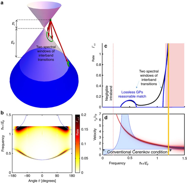
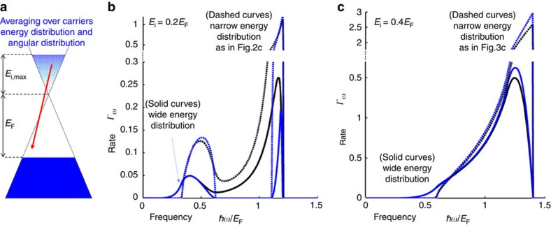
 with maximum hot carrier energy of Ei,max=0.2 eV corresponding to Fig. 2, or (c)
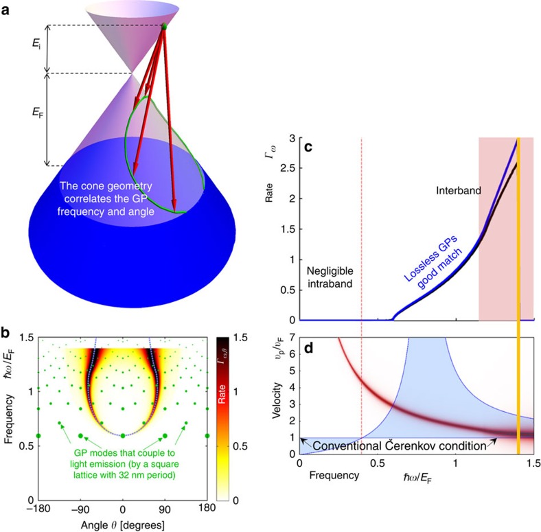
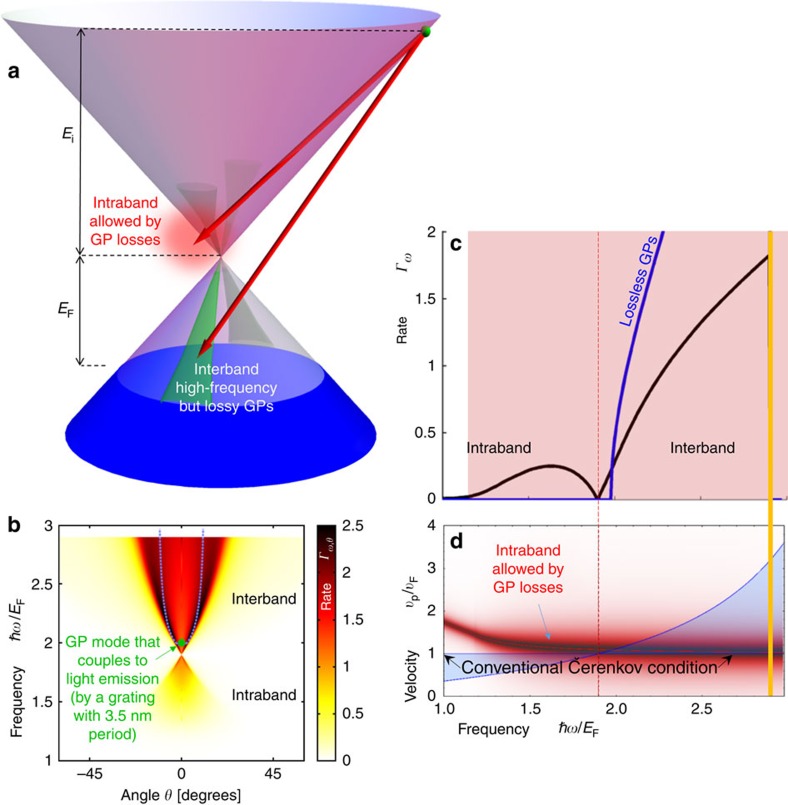
  with maximum hot carrier energy of Ei,max=0.4 eV corresponding to Fig. 3. In both b and c we plot the exact spectrum (integrating equation (6) over the energy distribution) in solid black and the lossless approximation (integrating equation (5) over the energy distribution) in solid blue. The dashed curves are for the respective cases of narrow energy distribution (matching Figs 2c and 3c). The Fermi energy EF is as in Figs 2, 3, 4.
Similar articles
-
Optical nano-imaging of gate-tunable graphene plasmons.Nature. 2012 Jul 5;487(7405):77-81. doi: 10.1038/nature11254. Nature. 2012. PMID: 22722861
-
Engineering Graphene Grain Boundaries for Plasmonic Multi-Excitation and Hotspots.ACS Nano. 2022 Jun 28;16(6):9041-9048. doi: 10.1021/acsnano.2c00396. Epub 2022 Jun 13. ACS Nano. 2022. PMID: 35696451
-
Nonlinear Graphene Nanoplasmonics.Acc Chem Res. 2019 Sep 17;52(9):2536-2547. doi: 10.1021/acs.accounts.9b00308. Epub 2019 Aug 26. Acc Chem Res. 2019. PMID: 31448890
-
Controlling graphene plasmons with a zero-index metasurface.Nanoscale. 2017 Nov 30;9(46):18482-18489. doi: 10.1039/c7nr05555b. Nanoscale. 2017. PMID: 29160326
-
Quantum Plasmonics: Energy Transport Through Plasmonic Gap.Adv Mater. 2021 Nov;33(47):e2006606. doi: 10.1002/adma.202006606. Epub 2021 Apr 23. Adv Mater. 2021. PMID: 33891781 Review.
Cited by
-
Interface nano-optics with van der Waals polaritons.Nature. 2021 Sep;597(7875):187-195. doi: 10.1038/s41586-021-03581-5. Epub 2021 Sep 8. Nature. 2021. PMID: 34497390 Review.
-
Imaging and controlling plasmonic interference fields at buried interfaces.Nat Commun. 2016 Oct 11;7:13156. doi: 10.1038/ncomms13156. Nat Commun. 2016. PMID: 27725670 Free PMC article.
-
Hyperbolic phonon-polariton electroluminescence in 2D heterostructures.Nature. 2025 Mar;639(8056):915-921. doi: 10.1038/s41586-025-08686-9. Epub 2025 Mar 19. Nature. 2025. PMID: 40108468
-
Control of quantum electrodynamical processes by shaping electron wavepackets.Nat Commun. 2021 Mar 17;12(1):1700. doi: 10.1038/s41467-021-21367-1. Nat Commun. 2021. PMID: 33731697 Free PMC article.
-
Timing Estimation and Limits in TOF-PET Detectors Producing Prompt Photons.IEEE Trans Radiat Plasma Med Sci. 2023 Sep;7(7):692-703. doi: 10.1109/trpms.2023.3279455. Epub 2023 May 24. IEEE Trans Radiat Plasma Med Sci. 2023. PMID: 38156329 Free PMC article.
References
-
- Fang Y. & Sun M. Nanoplasmonic waveguides: towards applications in integrated nanophotonic circuits. Light Sci. Appl. 4, 294 (2015).
-
- Atwater H. A. The promise of plasmonics. Sci. Am. 296, 56–62 (2007). - PubMed
-
- MacDonald K. F., Sámson Z. L., Stockman M. I. & Zheludev N. I. Ultrafast active plasmonics. Nat. Photonics 3, 55–58 (2009).
-
- Bharadwaj P., Bouhelier A. & Novotny L. Electrical excitation of surface plasmons. Phys. Rev. Lett. 106, 226802 (2011). - PubMed
-
- Koller D. M. et al. Organic plasmon-emitting diode. Nat. Photonics 2, 684–687 (2008).
Publication types
LinkOut - more resources
Full Text Sources
Other Literature Sources
