Geometrically pinned magnetic domain wall for multi-bit per cell storage memory
- PMID: 27334038
- PMCID: PMC4917858
- DOI: 10.1038/srep28590
Geometrically pinned magnetic domain wall for multi-bit per cell storage memory
Abstract
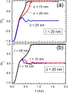
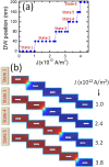
Spintronic devices currently rely on magnetic switching or controlled motion of domain walls (DWs) by an external magnetic field or a spin-polarized current. Controlling the position of DW is essential for defining the state/information in a magnetic memory. During the process of nanowire fabrication, creating an off-set of two parts of the device could help to pin DW at a precise position. Micromagnetic simulation conducted on in-plane magnetic anisotropy materials shows the effectiveness of the proposed design for pinning DW at the nanoconstriction region. The critical current for moving DW from one state to the other is strongly dependent on nanoconstricted region (width and length) and the magnetic properties of the material. The DW speed which is essential for fast writing of the data could reach values in the range of hundreds m/s. Furthermore, evidence of multi-bit per cell memory is demonstrated via a magnetic nanowire with more than one constriction.
Figures


Similar articles
-
Thermal Effects on Domain Wall Stability at Magnetic Stepped Nanowire for Nanodevices Storage.Nanomaterials (Basel). 2024 Jul 15;14(14):1202. doi: 10.3390/nano14141202. Nanomaterials (Basel). 2024. PMID: 39057879 Free PMC article.
-
Voltage control of magnetic domain wall injection into strain-mediated multiferroic heterostructures.Nanoscale. 2020 Jul 21;12(27):14479-14486. doi: 10.1039/d0nr02595j. Epub 2020 Jun 15. Nanoscale. 2020. PMID: 32538417
-
Control of domain wall pinning in ferromagnetic nanowires by magnetic stray fields.Nanotechnology. 2011 Feb 25;22(8):085201. doi: 10.1088/0957-4484/22/8/085201. Epub 2011 Jan 17. Nanotechnology. 2011. PMID: 21242625
-
Dynamic Manipulation of Chiral Domain Wall Spacing for Advanced Spintronic Memory and Logic Devices.ACS Nano. 2024 Jun 4;18(22):14507-14513. doi: 10.1021/acsnano.4c02024. Epub 2024 May 17. ACS Nano. 2024. PMID: 38758358 Free PMC article.
-
Progress in Spin Logic Devices Based on Domain-Wall Motion.Micromachines (Basel). 2024 May 24;15(6):696. doi: 10.3390/mi15060696. Micromachines (Basel). 2024. PMID: 38930666 Free PMC article. Review.
Cited by
-
Thermal Effects on Domain Wall Stability at Magnetic Stepped Nanowire for Nanodevices Storage.Nanomaterials (Basel). 2024 Jul 15;14(14):1202. doi: 10.3390/nano14141202. Nanomaterials (Basel). 2024. PMID: 39057879 Free PMC article.
-
A Micromagnetic Protocol for Qualitatively Predicting Stochastic Domain Wall Pinning.Sci Rep. 2017 Dec 19;7(1):17862. doi: 10.1038/s41598-017-17512-w. Sci Rep. 2017. PMID: 29259185 Free PMC article.
-
Optically Readable Multilevel Magnetic Memory States in Perpendicularly Exchange-Biased Ferromagnetic Multilayers.Small. 2025 Mar;21(10):e2411966. doi: 10.1002/smll.202411966. Epub 2025 Jan 26. Small. 2025. PMID: 39865923 Free PMC article.
References
-
- Parkin S. S. P., Hayashi M. & Thomas L. Magnetic domain-wall racetrack memory. Science 320, 190–194 (2008). - PubMed
-
- O’Brien L. et al.. Bidirectional magnetic nanowire shift register. Appl. Phys. Lett. 95, 232502 (2009).
-
- Diegel M., Glathe S., Mattheis R., Scherzinder M. & Halder E. A new four bit magnetic domain wall based multiturn counter. IEEE Trans. Magn. 45, 3792 (2009).
-
- Franken J. H., Swagten H. J. M. & Koopmans B. Shift registers based on magnetic domain wall ratchets with perpendicular anisotropy. Nat. Nanotechnol. 7, 499–503 (2012). - PubMed
-
- Tanigawa H. et al.. Thickness dependence of current-induced domain wall motion in a Co/Ni multi-layer with out-of-plane anisotropy. Appl. Phys. Lett. 102, 152410 (2013).
LinkOut - more resources
Full Text Sources
Other Literature Sources

