. 2016 Jun 23:6:28468.
doi: 10.1038/srep28468.

Spatially resolved photoresponse on individual ZnO nanorods: correlating morphology, defects and conductivity

Affiliations

Spatially resolved photoresponse on individual ZnO nanorods: correlating morphology, defects and conductivity

K Bandopadhyay et al. Sci Rep. .

Abstract

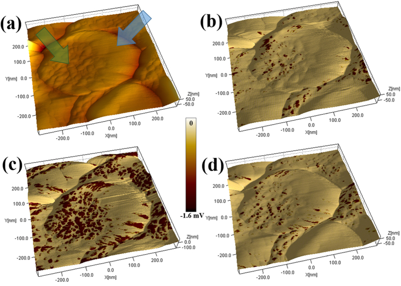
Electrically active native point defects have a significant impact on the optical and electrical properties of ZnO nanostructures. Control of defect distribution and a detailed understanding of their physical properties are central to designing ZnO in novel functional forms and architecture, which ultimately decides device performance. Defect control is primarily achieved by either engineering nanostructure morphology by tailoring growth techniques or doping. Here, we report conducting atomic force microscopy studies of spatially resolved photoresponse properties on ZnO nanorod surfaces. The photoresponse for super-band gap, ultraviolet excitations show a direct correlation between surface morphology and photoactivity localization. Additionally, the system exhibits significant photoresponse with sub-bandgap, green illumination; the signature energy associated with the deep level oxygen vacancy states. While the local current-voltage characteristics provide evidence of multiple transport processes and quantifies the photoresponse, the local time-resolved photoresponse data evidences large variations in response times (90 ms-50 s), across the surface of a nanorod. The spatially varied photoconductance and the range in temporal response display a complex interplay of morphology, defects and connectivity that brings about the true colour of these ZnO nanostructures.


Figures

Figure 1
Figure 1. Schematic of the atomic force microscope setup, modified with the optical fibre insert for illuminating the junction.
Figure 2
Figure 2
(a) SEM image of hexagonal ZnO nanorods (b) tapping mode AFM topography of nanorod surface; (c) CAFM topography and the simultaneously acquired current maps at sample bias of (d) −1.0 V (e) −1.5 V (f) −2.0 V. (current range in (d–f) are in 0 to −250 nA).
Figure 3
Figure 3
(a) Overlaid current map (at −2 V) on the 3D topography image of a ZnO nanorod. White circles demarcate areas of (1) low (2) medium and (3) high current. (b) Point IV characteristics recorded within the three current regions, the current values for (1) and (2) have been scaled by factors of 100 and 5 respectively, for clarity. Insets: (c) thermionic emission and (d) Fowler-Nordheim fits (see text) to forward bias IV data obtained at region 3.
Figure 4
Figure 4
(a) 3D topography image of a ZnO nanorod; the green and blue arrows indicate regions with smaller and larger grain structure. Corresponding dI/dV maps at (b) dark and upon (c) λ1 (355 nm) and (d) λ2 (532 nm) illumination.
Figure 5
Figure 5
(a) Topography of ZnO nanorod, (b,c) topography overlaid with CMAP for 355 and 532 nm excitation, (d,e) topography and CMAP line scans taken along white lines in (b,c), respectively. The blue and red arrows in (e) denote the grain centres and boundaries respectively.
Figure 6
Figure 6. Point IV spectra in dark and with λ1 (355 nm) and λ2 (532 nm) illuminations.
Inset shows the variation of junction conductance (dI/dV) with bias for the IV’s displayed.
Figure 7
Figure 7. Transient photoresponse of a single grain upon λ1 (355 nm) excitation at a sample bias of +300 mV.
Figure 8
Figure 8. Variation of the photoresponse rise and decay time constants with applied bias.
The error bars indicate the range of values obtained from photoresponse of various active grains.

Similar articles

Cited by

References

    1. Chen Z., Boya L., Junming Z., Guoping W. & Sheng C. Hybrid material based on plasmonic nanodisks decorated ZnO and its application on nanoscale lasers. Nanotechnology 25, 295203 (2014). - PubMed
    1. Lu J. et al.. Improved UV photoresponse of ZnO nanorod arrays by resonant coupling with surface plasmons of Al nanoparticles. Nanoscale 7, 3396–3403, 10.1039/C4NR07114J (2015). - DOI - PubMed
    1. Wang T., Lv R., Zhang P., Li C. & Gong J. Au nanoparticle sensitized ZnO nanopencil arrays for photoelectrochemical water splitting. Nanoscale, 10.1039/C4NR03735A (2014). - DOI - PubMed
    1. Zhang L. et al.. A High-Reliability Kevlar Fiber-ZnO Nanowires Hybrid Nanogenerator and its Application on Self-Powered UV Detection. Adv. Funct. Mater. 25, 5794–5798, 10.1002/adfm.201502646 (2015). - DOI
    1. Hu Y. et al.. Supersensitive, Fast-Response Nanowire Sensors by Using Schottky Contacts. Adv. Mater. 22, 3327–3332, 10.1002/adma.201000278 (2010). - DOI - PubMed

Publication types

LinkOut - more resources