. 2016 Jun 24:6:28669.
doi: 10.1038/srep28669.

Cloaking of solar cell contacts at the onset of Rayleigh scattering

Affiliations

Cloaking of solar cell contacts at the onset of Rayleigh scattering

Etor San Román et al. Sci Rep. .

Abstract

Electrical contacts on the top surface of solar cells and light emitting diodes cause shadow losses. The phenomenon of extraordinary optical transmission through arrays of subwavelength holes suggests the possibility of engineering such contacts to reduce the shadow using plasmonics, but resonance effects occur only at specific wavelengths. Here we describe instead a broadband effect of enhanced light transmission through arrays of subwavelength metallic wires, due to the fact that, in the absence of resonances, metal wires asymptotically tend to invisibility in the small size limit regardless of the fraction of the device area taken up by the contacts. The effect occurs for wires more than an order of magnitude thicker than the transparency limit for metal thin films. Finite difference in time domain calculations predict that it is possible to have high cloaking efficiencies in a broadband wavelength range, and we experimentally demonstrate contact shadow losses less than half of the geometric shadow.


Figures
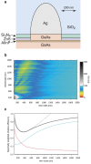
Figure 1
Figure 1. Shadow efficiency for silver wires on a GaAs solar cell.
(a) Structure used to calculate the optical losses caused by the top metal contact. (b) The fraction of the incoming power lost due to reflection and absorption at the metal contact is plotted normalized to the fraction of the area taken up by the contact as a function of wavelength and wire width. The wire height and period are fixed at 600 nm and 10 μm, respectively. Normal incidence illumination with unpolarized light. (c) Spectrally integrated shadow efficiency as a function of wire width. The data are weighted with the direct+ circumsolar AM1.5 solar spectrum. The red and blue lines represent, respectively, the absorption and reflection contributions to the total shadow (thick grey line). The dashed line is a fit to an ax + b/x expression with only two free parameters were the two terms can be identified with non-resonant Rayleigh extinction and resonant extinction, respectively.
Figure 2
Figure 2. Comparison of experimental and simulated results for silver and gold wire arrays.
(a) Scanning electron microscopy image of silver wires electrodeposited through a SiOx mask on a GaAs solar cell. The length of the scale bar is half the 4 μm array period. (b) Experimentally measured shadow efficiencies for the silver wires in Fig. 2a. Results for transversal polarization, parallel polarization, and unpolarized light are shown in orange, blue, and black, respectively. (c) FDTD simulations corresponding to the experimental results for silver wires in Fig. 2b. (d) Scanning electron microscopy image of gold wires electrodeposited through a SiOx mask on a GaAs solar cell. The length of the scale bar is twice the 16.7 μm array period. (e) Experimentally measured shadow efficiencies for gold wires. (f) FDTD simulations corresponding to the experimental results for gold wires.
Figure 3
Figure 3. Calculated power loss caused by the top contact.
The plot represents the ratio of the power loss to the device power output. Lighter to darker shades of blue correspond respectively to array periods of 20, 40, 60, 80, 100, 120 and 140 μm.
Figure 4
Figure 4. Metal nanowire array fabrication sequence.
(a) SiOx deposition by CVD. (b) Organic antireflective coating and photoresist spin coating. (c) Photoresist exposure by laser interference lithography. (d) Photoresist development. (e) Cr deposition. (f) Lift off. (g) Reactive ion etching. (h) Seed contact metal deposition by sputtering. (i) Organic antireflective coating lift off. (j) Electrodeposition. (k) Grazing angle Ar ion milling. (l) Finished contact array.

References

    1. Meulenberg A. The sawtooth coverslide-A new means of coupling light into solar cells. J. Energy 1, 151 (1977).
    1. Schumann M. F. et al.. Cloaked contact grids on solar cells by coordinate transformations: designs and prototypes. Optica 2, 850 (2015).
    1. Hsu P.-C. et al.. Performance enhancement of metal nanowire transparent conducting electrodes by mesoscale metal wires. Nature Comm. 4, 2114 (2013). - PubMed
    1. Wu H. et al.. A transparent electrode based on a metal nanotrough network. Nature Nanotech. 8, 421–425 (2013). - PubMed
    1. Van Beijnum F. et al.. Quasi-cylindrical wave in expericontribution ments on extraordinary optical transmission. Nature 492, 411 (2012). - PubMed

Publication types