Review
. 2016 Jun 30;60(1):81-90.
doi: 10.1042/EBC20150009.

Biologically sensitive field-effect transistors: from ISFETs to NanoFETs

Affiliations
Review

Biologically sensitive field-effect transistors: from ISFETs to NanoFETs

Vivek Pachauri et al. Essays Biochem. .

Abstract

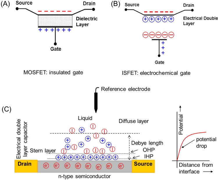
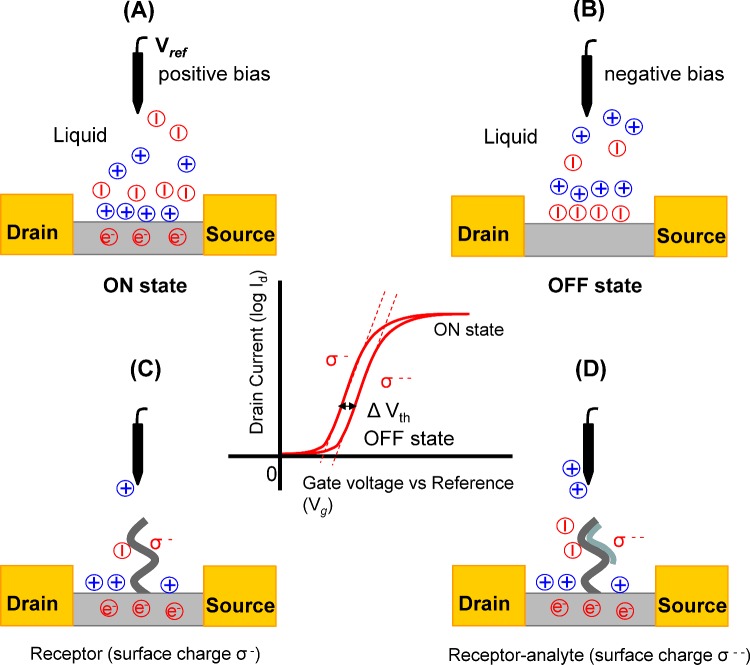
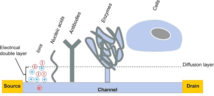
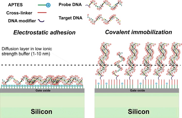
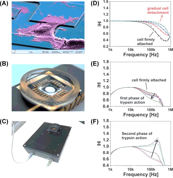
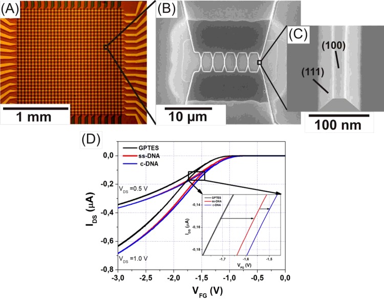
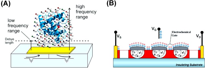
Biologically sensitive field-effect transistors (BioFETs) are one of the most abundant classes of electronic sensors for biomolecular detection. Most of the time these sensors are realized as classical ion-sensitive field-effect transistors (ISFETs) having non-metallized gate dielectrics facing an electrolyte solution. In ISFETs, a semiconductor material is used as the active transducer element covered by a gate dielectric layer which is electronically sensitive to the (bio-)chemical changes that occur on its surface. This review will provide a brief overview of the history of ISFET biosensors with general operation concepts and sensing mechanisms. We also discuss silicon nanowire-based ISFETs (SiNW FETs) as the modern nanoscale version of classical ISFETs, as well as strategies to functionalize them with biologically sensitive layers. We include in our discussion other ISFET types based on nanomaterials such as carbon nanotubes, metal oxides and so on. The latest examples of highly sensitive label-free detection of deoxyribonucleic acid (DNA) molecules using SiNW FETs and single-cell recordings for drug screening and other applications of ISFETs will be highlighted. Finally, we suggest new device platforms and newly developed, miniaturized read-out tools with multichannel potentiometric and impedimetric measurement capabilities for future biomedical applications.

Keywords: field-effect transistors; field-effect-based biosensors; silicon nanowire sensors.


Figures

Figure 1.
Figure 1.. Schematic representation of the operation principle of MOSFETs and ISFETs
(A) The three-electrode configuration in a MOSFET with a dielectric insulator material sandwiched between the channel and gate electrodes. (B) In transistors made from metal oxides or in graphene-based FETs the EDL can replace the high dielectric insulator material of the standard ISFET configuration. (C) Microscopic representation of the formation of the EDL and electrical double layer capacitance on a solid–liquid interface of an ISFET. IHP, inner Helmholtz plane; OHP, outer Helmholtz plane.
Figure 2.
Figure 2.. Principle of the operation of an ISFET- and FET-based transducer
(A and B) Applying positive and negative bias at the Ag/AgCl reference electrode change the polarity of the electrical double layer. (C and D) Change in the net charge-carrier density on an ISFET surface modified with a receptor biomolecule before and after binding with an analyte molecule. The change in the net surface charge shifts the field-effect curve as shown in the graph in the centre.
Figure 3.
Figure 3.. Schematic representation of a biologically sensitive ISFET and different types of analytes with variable sizes in relation to the thickness of the EDL (analyte size is not to scale)
Only DNA molecules present charges inside the EDL, whereas only fractions of the much larger antibody and enzyme molecules directly affect the EDL (only in the case of diluted buffer concentrations). In the case of cells, the cellular membrane is clearly outside this range, since typical average distances between the cellular membrane and the surface are in the range 50–100 nm.
Figure 4.
Figure 4.. Different strategies for the immobilization of probe DNA
On the left, the DNA molecules are attached to the aminosilane layer by electrostatic immobilization. This usually leads to high FET signal amplitudes for the immobilization process because the oligonucleotides are very closely attached to the gate oxide. The hybridization efficiency, however, is not very high in these experiments. On the right, the probe single-stranded DNA (ssDNA) is covalently attached utilizing a cross-linker in combination with end-functionalized ssDNA. Generally, the double-stranded molecules are stiffer and longer compared with the unoccupied ssDNA molecules. For alternative silane layers other cross-linkers and covalent linking strategies are used.
Figure 5.
Figure 5.. Monitoring of the influence of cell-related parameters at a single-cell level using impedance spectra measured with silicon-based BioFETs
(A) A human embryonic kidney (HEK)-293 cell sitting on top of the BioFETs. (B and C) The cell-culture chamber on top of the silicon chip and the miniaturized measurement platform. (DF) The transfer function spectra after cells were treated with trypsin while following the cell-detachment process over time [29].
Figure 6.
Figure 6.. Detection of immobilized DNA on SiNW FETs
(AC) A high-density SiNW FET chip with a detailed structural view taken by scanning electron microscopy. (D) Transfer characteristics before (left curve) and after DNA immobilization (middle curve), and after hybridization (right curve). DNA was site-selectively immobilized on some channels of the array using a micro-spotter. Depending on the grafting density of the molecules and on the hybridization efficiency typical shifts of 10–200 mV are recorded with the silicon nanowire devices. This is much larger than typical signals recorded with ISFETs [42].
Figure 7.
Figure 7.. CMOS nanocapacitors (A) and ISMESFETs (B) are new concepts in measurement methods and device architectures

Similar articles

Cited by

References

    1. Nishi Y., Doering R. Handbook of Semiconductor Manufacturing Technology. 2nd edn. Boca Raton: CRC Press; 2007.
    1. Besselink G.A.L., Bergveld P. ISFET affinity sensor. In: Rogers K.R., Mulchandani A., editors. Affinity Biosensors: Techniques and Protocols. Totowa: Springer Humana Press; 1998. pp. 173–185.
    1. Sze S.M., Ng K.K. Physics of Semiconductor Devices. 3rd edn. Hoboken: Wiley; 2006.
    1. Zhang G-J., Chua J.H., Chee R-E., Agarwal A., Wong S.M., Buddharaju K.D., et al. Highly sensitive measurements of PNA-DNA hybridization using oxide-etched silicon nanowire biosensors. Biosens. Bioelectron. 2008;23:1701–1707. doi: 10.1016/j.bios.2008.02.006. - DOI - PubMed
    1. Thirsk H.R., Rangarajan S.K. The electrical double layer. Electrochemistry. 1980;7:203–256. doi: 10.1039/2050-9413. - DOI

Publication types

MeSH terms

Substances