

Monolayer MoS2 Bandgap Modulation by Dielectric Environments and Tunable Bandgap Transistors
- PMID: 27378032
- PMCID: PMC4932597
- DOI: 10.1038/srep29184
Monolayer MoS2 Bandgap Modulation by Dielectric Environments and Tunable Bandgap Transistors
Abstract
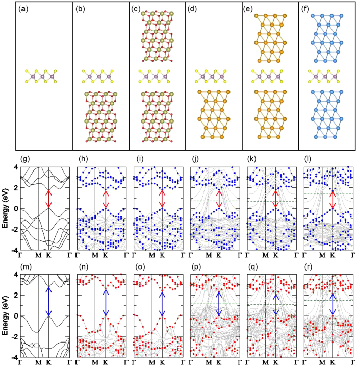
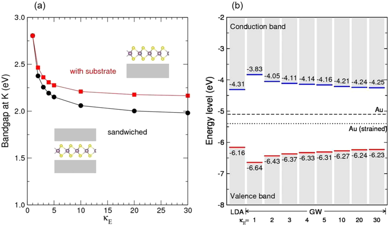
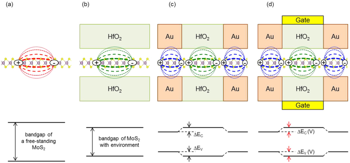
Semiconductors with a moderate bandgap have enabled modern electronic device technology, and the current scaling trends down to nanometer scale have introduced two-dimensional (2D) semiconductors. The bandgap of a semiconductor has been an intrinsic property independent of the environments and determined fundamental semiconductor device characteristics. In contrast to bulk semiconductors, we demonstrate that an atomically thin two-dimensional semiconductor has a bandgap with strong dependence on dielectric environments. Specifically, monolayer MoS2 bandgap is shown to change from 2.8 eV to 1.9 eV by dielectric environment. Utilizing the bandgap modulation property, a tunable bandgap transistor, which can be in general made of a two-dimensional semiconductor, is proposed.
Figures
References
-
- Radisavljevic B., Radenovic A., Brivio J., Giacometti V. & Kis A. Single-layer MoS2 transistors. Nat. Nanotechnol. 6, 147–150 (2011). - PubMed
-
- Radisavljevic B. & Kis A. Mobility engineering and a metal–insulator transition in monolayer MoS2. Nat. Mater. 12, 815–820 (2013). - PubMed
-
- Jena D. & Knar A. Enhancement of carrier mobility in semiconductor nanostructures by dielectric engineering. Phys. Rev. Lett. 98, 136805 (2007). - PubMed
-
- Noh J.-Y., Kim H., Park M. & Kim Y.-S. Deep-to-shallow level transition of Re and Nb dopants in monolayer MoS2 with dielectric environments. Phys. Rev. B 92, 115431 (2015).
Publication types
LinkOut - more resources
Full Text Sources
Other Literature Sources
