Enhanced optoelectronic performances of vertically aligned hexagonal boron nitride nanowalls-nanocrystalline diamond heterostructures
- PMID: 27404130
- PMCID: PMC4941520
- DOI: 10.1038/srep29444
Enhanced optoelectronic performances of vertically aligned hexagonal boron nitride nanowalls-nanocrystalline diamond heterostructures
Abstract
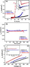
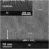
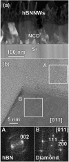
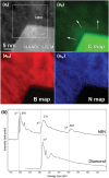
Field electron emission (FEE) properties of vertically aligned hexagonal boron nitride nanowalls (hBNNWs) grown on Si have been markedly enhanced through the use of nitrogen doped nanocrystalline diamond (nNCD) films as an interlayer. The FEE properties of hBNNWs-nNCD heterostructures show a low turn-on field of 15.2 V/μm, a high FEE current density of 1.48 mA/cm(2) and life-time up to a period of 248 min. These values are far superior to those for hBNNWs grown on Si substrates without the nNCD interlayer, which have a turn-on field of 46.6 V/μm with 0.21 mA/cm(2) FEE current density and life-time of 27 min. Cross-sectional TEM investigation reveals that the utilization of the diamond interlayer circumvented the formation of amorphous boron nitride prior to the growth of hexagonal boron nitride. Moreover, incorporation of carbon in hBNNWs improves the conductivity of hBNNWs. Such a unique combination of materials results in efficient electron transport crossing nNCD-to-hBNNWs interface and inside the hBNNWs that results in enhanced field emission of electrons. The prospective application of these materials is manifested by plasma illumination measurements with lower threshold voltage (370 V) and longer life-time, authorizing the role of hBNNWs-nNCD heterostructures in the enhancement of electron emission.
Figures


References
-
- De Heer W. A., Chatelain A. & Ugarte D. A Carbon nanotube field-emission electron source. Science 270, 1179–1180 (1995).
-
- Teo K. B. K. et al.. Field emission from dense, sparse, and patterned arrays of carbon nanofibers. Appl. Phys. Lett. 80, 2011–2013 (2002).
-
- Wei W. et al.. LaB6 tip-modified multiwalled carbon nanotubes as high quality field emission electron source. Appl. Phys. Lett. 89, 203112 (2006).
-
- Baughman R. H., Zakhidov A. A. & de Heer W. A. Carbon nanotubes-the route toward applications. Science 297, 787–792 (2002). - PubMed
-
- Hernandez-Garcia C., Stutzman M. L. & Oshea P. G. Electron sources for accelerators. Phys. Today 61, 44–49 (2008).
Publication types
LinkOut - more resources
Full Text Sources
Other Literature Sources

