Spontaneous formation of spiral-like patterns with distinct periodic physical properties by confined electrodeposition of Co-In disks
- PMID: 27462025
- PMCID: PMC4961954
- DOI: 10.1038/srep30398
Spontaneous formation of spiral-like patterns with distinct periodic physical properties by confined electrodeposition of Co-In disks
Abstract
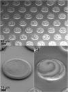
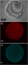
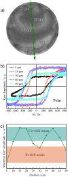
Spatio-temporal patterns are ubiquitous in different areas of materials science and biological systems. However, typically the motifs in these types of systems present a random distribution with many possible different structures. Herein, we demonstrate that controlled spatio-temporal patterns, with reproducible spiral-like shapes, can be obtained by electrodeposition of Co-In alloys inside a confined circular geometry (i.e., in disks that are commensurate with the typical size of the spatio-temporal features). These patterns are mainly of compositional nature, i.e., with virtually no topographic features. Interestingly, the local changes in composition lead to a periodic modulation of the physical (electric, magnetic and mechanical) properties. Namely, the Co-rich areas show higher saturation magnetization and electrical conductivity and are mechanically harder than the In-rich ones. Thus, this work reveals that confined electrodeposition of this binary system constitutes an effective procedure to attain template-free magnetic, electric and mechanical surface patterning with specific and reproducible shapes.
Figures


References
-
- Cui S. et al.. Hybrid plasmonic photonic crystal cavity for enhancing emission from near-surface nitrogen vacancy centers in diamond. ACS Photonics 2, 465–469 (2015).
-
- Zhou X., Boey F., Huo F., Huang L. & Zhang H. Chemically functionalized surface patterning. Small 7, 2273–2289 (2011). - PubMed
-
- Chen Y. Nanofabrication by electron beam lithography and its applications: A review. Microelectron. Eng. 135, 57–72 (2015).
-
- Vazquez-Mena O. et al.. Resistless nanofabrication by stencil lithography: A review. Microelectron. Eng. 132, 236–254 (2015).
Publication types
MeSH terms
Substances
LinkOut - more resources
Full Text Sources
Other Literature Sources

