. 2016 Dec;11(1):355.
doi: 10.1186/s11671-016-1567-6. Epub 2016 Aug 4.

Optimizing Silicon Oxide Embedded Silicon Nanocrystal Inter-particle Distances

Affiliations

Optimizing Silicon Oxide Embedded Silicon Nanocrystal Inter-particle Distances

Martijn van Sebille et al. Nanoscale Res Lett. 2016 Dec.

Abstract

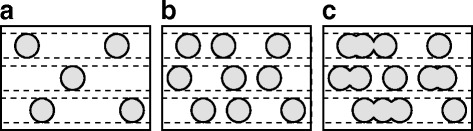
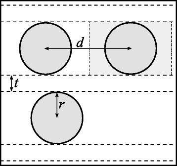
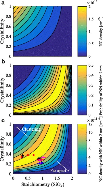
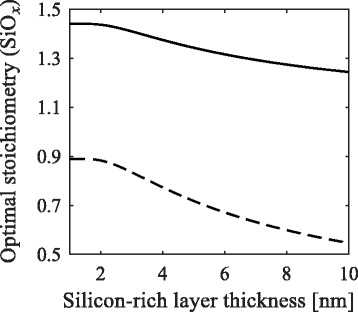
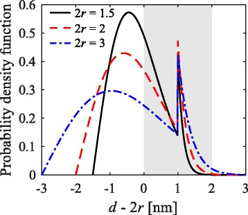
We demonstrate an analytical method to optimize the stoichiometry and thickness of multilayer silicon oxide films in order to achieve the highest density of non-touching and closely spaced silicon nanocrystals after annealing. The probability of a nanocrystal nearest-neighbor distance within a limited range is calculated using the stoichiometry of the as-deposited film and the crystallinity of the annealed film as input parameters. Multiplying this probability with the nanocrystal density results in the density of non-touching and closely spaced silicon nanocrystals. This method can be used to estimate the best as-deposited stoichiometry in order to achieve optimal nanocrystal density and spacing after a subsequent annealing step.

Keywords: Inter-particle distance; Silicon nanocrystal; Silicon oxide; Spacing; Stoichiometry.


Figures

Fig. 1
Fig. 1
Nanocrystal spacing and clustering. Nanocrystals formed in silicon-rich layers with relatively low (a), medium (b), and high (c) excess silicon, separated by stoichiometric buffer layers
Fig. 2
Fig. 2
Nanocrystals in a multilayer structure shown schematically. Nanocrystals in a multilayer structure shown schematically, including the nanocrystal radius r, buffer layer thickness t, and inter-particle distance d. The enclosing box around a nanocrystal is shown for the right-hand nanocrystal
Fig. 3
Fig. 3
TEM image of a multilayer sample and its nanocrystal diameter histogram. a Cross-sectional high-resolution TEM image of an annealed multilayer sample with silicon-rich and buffer layer thicknesses of 3 and 1 nm, respectively. b The histogram of the sample’s nanocrystal diameters. Approximately 250 nanocrystals were measured. The histogram is fitted with a log-normal probability density function with μ= 0.83 nm and σ= 0.27 nm
Fig. 4
Fig. 4
Nanocrystal diameter in a multilayer sample as a function of the silicon-rich layer thickness. The mean nanocrystal diameter D¯ (solid symbols) and the mean equivalent diameter D¯equiv (open symbols) for samples with varying silicon-rich layer thicknesses. The black data points are obtained from Gutsch et al. [18]. The dashed line represents the equality between the nanocrystal diameter and the silicon-rich layer thickness
Fig. 5
Fig. 5
Nanocrystal density, NN probability, and NN density. The 2D nanocrystal (NC) density (a), the probability of finding a nearest neighbor (NN) within 2 nm (b), and the density of nanocrystals with a NN within 2 nm (c) as a function of the silicon-rich layer composition and crystallinity for a sample with silicon-rich and buffer layer thicknesses of 3 and 1 nm, respectively. The black diamonds represent tube furnace annealed intrinsic samples. The red, magenta, and blue squares show intrinsic, p-type and n-type samples annealed using RTA
Fig. 6
Fig. 6
Optimal stoichiometry. The optimal stoichiometry for films with varying silicon-rich layer thicknesses for a sample with crystallinity of 1 (solid line) and 0.4 (dashed line). The buffer layer thickness is kept constant at 1 nm
Fig. 7
Fig. 7
Nearest-neighbor distance probability density functions. The nearest-neighbor distance probability density functions for samples with silicon-rich layer thicknesses of 1.5, 2, and 3 nm and buffer layer thickness of 1 nm, calculated using their respective optimal compositions. The gray area depicts the range of desired nearest-neighbor distances. Shorter distances imply clustering, and greater distances lead to an insufficient tunneling probability

References

    1. Green MA, Cho EC, Cho Y, Huang Y, Pink E, Trupke T, Lin A, Fangsuwannarak T, Puzzer T, Conibeer G, Corkish R (2005) All-silicon tandem cells based on artificial semiconductor synthesised using silicon quantum dots in a dielectric matrix In: Proceedings of the 20th European Photovoltaic Solar Energy Conference and Exhibition, 3–7.
    1. Heitmann J, Müller F, Zacharias M, Gösele U. Silicon nanocrystals: size matters. Adv Mater. 2005;17(7):795–803. doi: 10.1002/adma.200401126. - DOI
    1. Künle M, Kaltenbach T, Löper P, Hartel A, Janz S, Eibl O, Nickel KG. Si-rich a-SiC:H thin films: structural and optical transformations during thermal annealing. Thin Solid Films. 2010;519(1):151–157. doi: 10.1016/j.tsf.2010.07.085. - DOI
    1. Puthen-Veettil B, Patterson R, König D, Conibeer G, Green MA. The impact of disorder on charge transport in three dimensional quantum dot resonant tunneling structures. J Appl Phys. 2014;116(16):163707. doi: 10.1063/1.4899207. - DOI
    1. Schnabel M, Weiss C, Löper P, Wilshaw PR, Janz S. Self-assembled silicon nanocrystal arrays for photovoltaics. Phys Stat Solidi A. 2015;212(8):1649–1661. doi: 10.1002/pssa.201431764. - DOI

LinkOut - more resources