

Nanometal Skin of Plasmonic Heterostructures for Highly Efficient Near-Field Scattering Probes
- PMID: 27502178
- PMCID: PMC4977468
- DOI: 10.1038/srep31113
Nanometal Skin of Plasmonic Heterostructures for Highly Efficient Near-Field Scattering Probes
Abstract
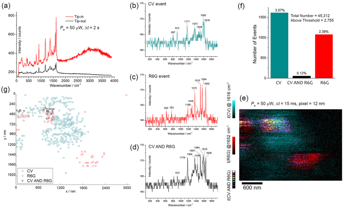
In this work, atomic force microscopy probes are functionalized by virtue of self-assembling monolayers of block copolymer (BCP) micelles loaded either with clusters of silver nanoparticles or bimetallic heterostructures consisting of mixed species of silver and gold nanoparticles. The resulting self-organized patterns allow coating the tips with a sort of nanometal skin made of geometrically confined nanoislands. This approach favors the reproducible engineering and tuning of the plasmonic properties of the resulting structured tip by varying the nanometal loading of the micelles. The newly conceived tips are applied for experiments of tip-enhanced Raman scattering (TERS) spectroscopy and scattering-type scanning near-field optical microscopy (s-SNOM). TERS and s-SNOM probe characterizations on several standard Raman analytes and patterned nanostructures demonstrate excellent enhancement factor with the possibility of fast scanning and spatial resolution <12 nm. In fact, each metal nanoisland consists of a multiscale heterostructure that favors large scattering and near-field amplification. Then, we verify the tips to allow challenging nongap-TER spectroscopy on thick biosamples. Our approach introduces a synergistic chemical functionalization of the tips for versatile inclusion and delivery of plasmonic nanoparticles at the tip apex, which may promote the tuning of the plasmonic properties, a large enhancement, and the possibility of adding new degrees of freedom for tip functionalization.
Figures
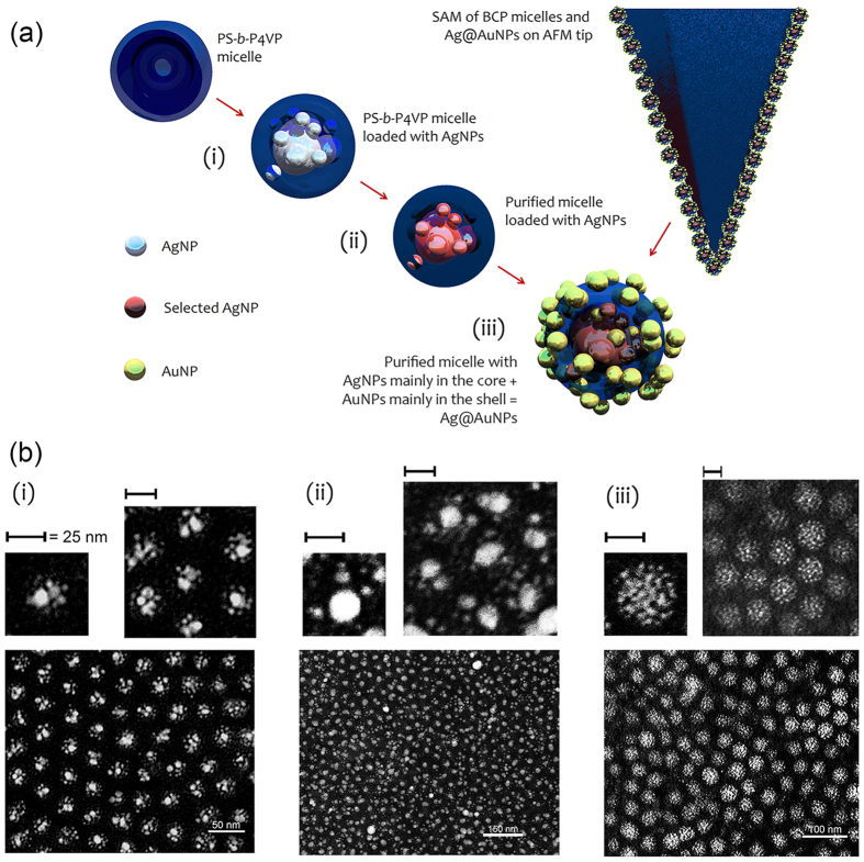
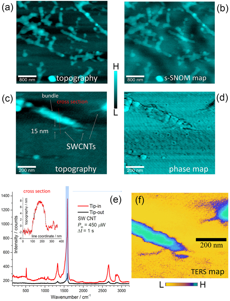
 as Ag@AuNPs). Finally, both solutions of BCP with AgNPs or Ag@AuNPs are used to coat Si-AFM tips by dip coating. (b) TEM micrographs (inverted colormap) of the three steps of the process depicted in panel (a). In particular, the modification of the size of the NPs, evident from the comparison of the consecutive SAMs spin-coated on glass, pointed out the formation of AgNPs of 15–20 nm surrounded by smaller Ag seed satellites in the P4VP core (ii). An outer shell that we ascribe to tiny AuNPs (
 nm) appears in (iii) as described in the main text. Top insets are magnified regions of the corresponding bottom scans. Scalebars are 50, 150 and 100 nm in (i), (ii) and (iii), respectively, whereas scalebar = 25 nm in all top insets.
Similar articles
-
Optical antennas with multiple plasmonic nanoparticles for tip-enhanced Raman microscopy.Nanoscale. 2015 Nov 7;7(41):17424-33. doi: 10.1039/c5nr05022g. Nanoscale. 2015. PMID: 26439510
-
Tuning Localized Surface Plasmon Resonance in Scanning Near-Field Optical Microscopy Probes.ACS Nano. 2015 Jun 23;9(6):6297-304. doi: 10.1021/acsnano.5b01794. Epub 2015 Jun 9. ACS Nano. 2015. PMID: 26027751
-
Dielectrophoretic positioning of single nanoparticles on atomic force microscope tips for tip-enhanced Raman spectroscopy.Electrophoresis. 2015 May;36(9-10):1142-8. doi: 10.1002/elps.201400530. Electrophoresis. 2015. PMID: 25781418
-
Nanoscale Optical Microscopy and Spectroscopy Using Near-Field Probes.Annu Rev Chem Biomol Eng. 2018 Jun 7;9:365-387. doi: 10.1146/annurev-chembioeng-060817-084150. Epub 2018 Mar 29. Annu Rev Chem Biomol Eng. 2018. PMID: 29596000 Review.
-
Nanoscale chemical imaging using tip-enhanced Raman spectroscopy: a critical review.Angew Chem Int Ed Engl. 2013 Jun 3;52(23):5940-54. doi: 10.1002/anie.201203849. Epub 2013 Apr 22. Angew Chem Int Ed Engl. 2013. PMID: 23610002 Review.
Cited by
-
Sandwiching analytes with structurally diverse plasmonic nanoparticles on paper substrates for surface enhanced Raman spectroscopy.RSC Adv. 2019 Oct 11;9(56):32535-32543. doi: 10.1039/c9ra05399a. eCollection 2019 Oct 10. RSC Adv. 2019. PMID: 35529713 Free PMC article.
-
Liquid Phase Infiltration of Block Copolymers.Polymers (Basel). 2022 Oct 14;14(20):4317. doi: 10.3390/polym14204317. Polymers (Basel). 2022. PMID: 36297895 Free PMC article. Review.
-
Gold Nanoparticle Self-Aggregation on Surface with 1,6-Hexanedithiol Functionalization.Nanomaterials (Basel). 2020 Mar 11;10(3):512. doi: 10.3390/nano10030512. Nanomaterials (Basel). 2020. PMID: 32168942 Free PMC article.
-
Exploring Reliable and Efficient Plasmonic Nanopatterning for Surface- and Tip-Enhanced Raman Spectroscopies.Int J Mol Sci. 2023 Nov 10;24(22):16164. doi: 10.3390/ijms242216164. Int J Mol Sci. 2023. PMID: 38003354 Free PMC article. Review.
-
Spectroscopic Imaging at the Nanoscale: Technologies and Recent Applications.Anal Chem. 2018 Jan 2;90(1):440-458. doi: 10.1021/acs.analchem.7b04151. Epub 2017 Oct 27. Anal Chem. 2018. PMID: 29028297 Free PMC article. Review.
References
-
- Stöckle R. M., Suh Y. D., Deckert V. & Zenobi R. Nanoscale chemical analysis by tip-enhanced raman spectroscopy. Chem. Phys. Lett. 318, 131–136 (2000).
-
- Zhang R. et al.. Chemical mapping of a single molecule by plasmon-enhanced Raman scattering. Nature 498, 82–86 (2013). - PubMed
-
- De Angelis F. et al.. Nanoscale chemical mapping using three-dimensional adiabatic compression of surface plasmon polaritons. Nat. Nanotech. 5, 67–72 (2010). - PubMed
-
- Van Schrojenstein Lantman E. M., Deckert-Gaudig T., Mank A. J. G., Deckert V. & Weckhuysen B. M. Catalytic processes monitored at the nanoscale with tip-enhanced Raman spectroscopy. Nat. Nanotech. 7, 583–586 (2012). - PubMed
Publication types
LinkOut - more resources
Full Text Sources
Other Literature Sources
Miscellaneous
