

Resonant Zener tunnelling via zero-dimensional states in a narrow gap diode
- PMID: 27535896
- PMCID: PMC4989182
- DOI: 10.1038/srep32039
Resonant Zener tunnelling via zero-dimensional states in a narrow gap diode
Abstract
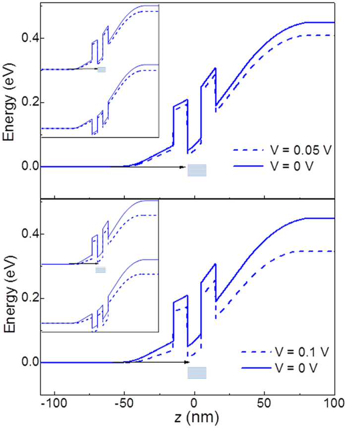
Interband tunnelling of carriers through a forbidden energy gap, known as Zener tunnelling, is a phenomenon of fundamental and technological interest. Its experimental observation in the Esaki p-n semiconductor diode has led to the first demonstration and exploitation of quantum tunnelling in a condensed matter system. Here we demonstrate a new type of Zener tunnelling that involves the resonant transmission of electrons through zero-dimensional (0D) states. In our devices, a narrow quantum well of the mid-infrared (MIR) alloy In(AsN) is placed in the intrinsic (i) layer of a p-i-n diode. The incorporation of nitrogen in the quantum well creates 0D states that are localized on nanometer lengthscales. These levels provide intermediate states that act as "stepping stones" for electrons tunnelling across the diode and give rise to a negative differential resistance (NDR) that is weakly dependent on temperature. These electron transport properties have potential for the development of nanometre-scale non-linear components for electronics and MIR photonics.
Figures


References
-
- Zener C. A. Theory of the Electrical Breakdown of Solid Dielectrics. Proc. R. Soc. London 145, 523 (1934).
-
- Esaki L. New Phenomenon in Narrow Germanium p-n Junctions. Phys. Rev. 109, 603 (1958).
-
- Katsnelson M. I., Novoselov K. S. & Geim A. K. Chiral tunneling and the Klein paradox in graphene. Nature Phys. 2, 620 (2006).
-
- Klein O. Die Reflexion von Elektronen an einem Potentialsprung nach der relativistischen Dynamik von Dirac. Z. Phys. 53, 157 (1929).
-
- Albrecht S. M. et al.. Exponential protection of zero modes in Majorana islands. Nature 531, 206 (2016). - PubMed
Publication types
LinkOut - more resources
Full Text Sources
Other Literature Sources
Miscellaneous
