

High Density Crossbar Arrays with Sub- 15 nm Single Cells via Liftoff Process Only
- PMID: 27585643
- PMCID: PMC5009344
- DOI: 10.1038/srep32614
High Density Crossbar Arrays with Sub- 15 nm Single Cells via Liftoff Process Only
Abstract
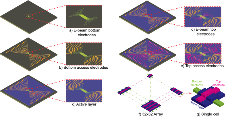
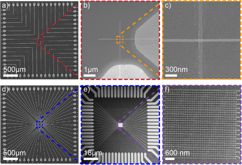
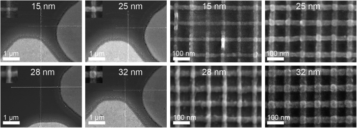
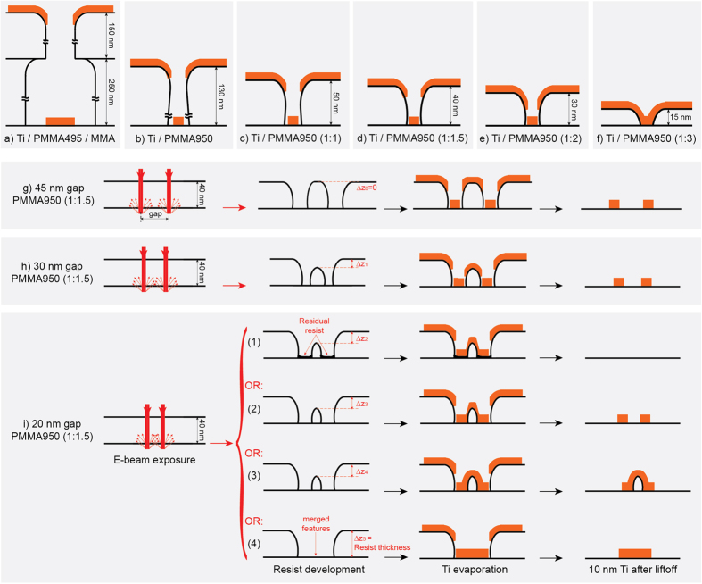
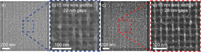
Emerging nano-scale technologies are pushing the fabrication boundaries at their limits, for leveraging an even higher density of nano-devices towards reaching 4F(2)/cell footprint in 3D arrays. Here, we study the liftoff process limits to achieve extreme dense nanowires while ensuring preservation of thin film quality. The proposed method is optimized for attaining a multiple layer fabrication to reliably achieve 3D nano-device stacks of 32 × 32 nanowire arrays across 6-inch wafer, using electron beam lithography at 100 kV and polymethyl methacrylate (PMMA) resist at different thicknesses. The resist thickness and its geometric profile after development were identified to be the major limiting factors, and suggestions for addressing these issues are provided. Multiple layers were successfully achieved to fabricate arrays of 1 Ki cells that have sub- 15 nm nanowires distant by 28 nm across 6-inch wafer.
Figures
References
-
- Zhong Z., Wang D., Cui Y., Bockrath M. W. & Lieber C. M. Nanowire Crossbar Arrays as Address Decoders for Integrated Nanosystems. Science (80-). 302, 1377–1379 (2003). - PubMed
-
- Chua L. O. Memristor-The Missing Circuit Element. IEEE Trans. Circuit Theory Ct-18, 507–519 (1971).
-
- Strukov D. B., Snider G. S., Stewart D. R. & Williams R. S. The missing memristor found. Nature 453, 80–83 (2008). - PubMed
-
- Chen W. & Ahmed H. Fabrication of 5–7 nm wide etched lines in silicon using 100 keV electron-beam lithography and polymethylmethacrylate resist. Appl. Phys. Lett. 62, 1499–1501 (1993).
-
- Yasin S., Hasko D. G. & Ahmed H. Fabrication of <5 nm width lines in poly(methylmethacrylate) resist using a water:isopropyl alcohol developer and ultrasonically-assisted development. Appl. Phys. Lett. 78, 2760–2762 (2001).
Publication types
LinkOut - more resources
Full Text Sources
Other Literature Sources
