. 2016 Sep 7:6:31932.
doi: 10.1038/srep31932.

Physical Realization of a Supervised Learning System Built with Organic Memristive Synapses

Affiliations

Physical Realization of a Supervised Learning System Built with Organic Memristive Synapses

Yu-Pu Lin et al. Sci Rep. .

Abstract

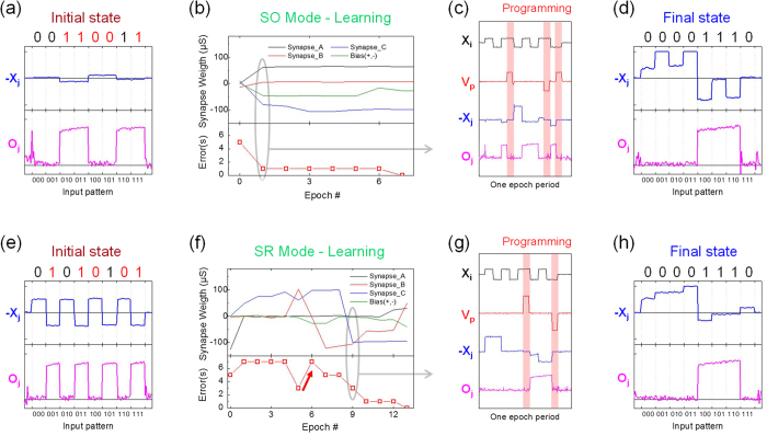
Multiple modern applications of electronics call for inexpensive chips that can perform complex operations on natural data with limited energy. A vision for accomplishing this is implementing hardware neural networks, which fuse computation and memory, with low cost organic electronics. A challenge, however, is the implementation of synapses (analog memories) composed of such materials. In this work, we introduce robust, fastly programmable, nonvolatile organic memristive nanodevices based on electrografted redox complexes that implement synapses thanks to a wide range of accessible intermediate conductivity states. We demonstrate experimentally an elementary neural network, capable of learning functions, which combines four pairs of organic memristors as synapses and conventional electronics as neurons. Our architecture is highly resilient to issues caused by imperfect devices. It tolerates inter-device variability and an adaptable learning rule offers immunity against asymmetries in device switching. Highly compliant with conventional fabrication processes, the system can be extended to larger computing systems capable of complex cognitive tasks, as demonstrated in complementary simulations.


Figures

Figure 1
Figure 1
Schematic representation of the neuromorphic learning system.
Figure 2
Figure 2
(a) Schematic representation of the metal/organic/metal memristor and the organic-composing active layer. (b) SEM image of the actual devices. Scale bar in the left and right images represent 20 μm and 200 nm, respectively. (c) Electrical characteristics of the memristor under voltage sweeps. (d) Top panel: Conductivity (G) evolution of the device under pulses with increasing amplitude. Gray traces show all transitions and one characteristic transition (black) is highlighted. Bottom panel: amplitude of each pulse. Inset: representation of the applied waveform. (e) Top panel: Statistics of conductivity change (ΔG) versus pulse amplitudes. The gray boxes show the 25–75% probability and the whiskers are 10–90%; bottom panel: SET/RESET event (ΔG/G0 > 40%) probability with respect to the pulse amplitude.
Figure 3
Figure 3
(a) A schematic of SO programming in an active case; while both possible correcting pulses are shown on the line, only one would be sent corresponding to depicted error case (b) Similar schematic showing SR programming being used to correct an error. (c) A diagram of device conductance evolution as it relates to appropriate thresholds for programming pulses in both modes. (d) Color-coded table of the active steps that SO programming implements. (e) Color-coded table of SR programming that implements all active steps. (f) Table which shows input, expected, line output, and prescribed weight change binary (sign) values at each of the four active steps.
Figure 4
Figure 4
Top row: Learning of “A nand B and C” function (00001110) using the SO programming mode. Bottom row: Learning of the same function using the SR programming mode. (a,e) Output of I-to-V converter (blue line, -Xj) and comparator (pink line, Oj) showing the initial state of the system of each learning. The initial errors are marked in red. (b,f) Learning histogram showing the synaptic weights (top panel) and total errors (bottom panel) evolution at each epoch. (c,g) Example of a single learning epoch (marked with grey circle in (b,f)) showing the input Xi (black), programming pulses at Yj (red), synaptic output -Xj of the I-to-V converter (blue), and digital output of the comparator Oj (pink) which is being compared to Yj. The active programming steps, when the system attempt to correct an error, are shaded red. (d,h) System output at the end of the learning, showing successful learning of the “A nand B and C” function.
Figure 5
Figure 5
(a) Threshold voltages variability of 11 memristors in the same chip (Vt1 in black and Vt2 in red). (b) Maximum and minimum conductivity (GMax, GMin) variation of these 11 devices. The symbols marks the average values and the error bars indicate their standard deviations. (c) Evolution of SET and RESET events in numbers of On/Off cycles, extracted from the data shown in Fig. 2d. The green line shows the moving average of Vt1, and the red line for the Vt2. (d) Contour map of SET and RESET voltage with respect to their initial conductivities, G0.

References

    1. Horowitz M. 1.1 computing’s energy problem (and what we can do about it). In 2014 IEEE International Solid-State Circuits Conference Digest of Technical Papers (ISSCC) 10–14 (2014).
    1. McCulloch W. S. & Pitts W. A logical calculus of the ideas immanent in nervous activity. The bulletin of mathematical biophysics 5, 115–133 (1943). - PubMed
    1. Jo S. H. et al.. Nanoscale memristor device as synapse in neuromorphic systems. Nano Letters 10, 1297–1301 (2010). - PubMed
    1. Chang T., Yang Y. & Lu W. Building neuromorphic circuits with memristive devices. IEEE Circuits and Systems Magazine 13, 56–73 (2013).
    1. Indiveri G., Linares-Barranco B., Legenstein R., Deligeorgis G. & Prodromakis T. Integration of nanoscale memristor synapses in neuromorphic computing architectures. Nanotechnology 24, 384010 (2013). - PubMed

Publication types

LinkOut - more resources