Material gain engineering in GeSn/Ge quantum wells integrated with an Si platform
- PMID: 27686056
- PMCID: PMC5043186
- DOI: 10.1038/srep34082
Material gain engineering in GeSn/Ge quantum wells integrated with an Si platform
Abstract
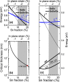
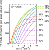
It is shown that compressively strained Ge1-xSnx/Ge quantum wells (QWs) grown on a Ge substrate with 0.1 ≤ x ≤ 0.2 and width of 8 nm ≤ d ≤ 14 nm are a very promising gain medium for lasers integrated with an Si platform. Such QWs are type-I QWs with a direct bandgap and positive transverse electric mode of material gain, i.e. the modal gain. The electronic band structure near the center of Brillouin zone has been calculated for various Ge1-xSnx/Ge QWs with use of the 8-band kp Hamiltonian. To calculate the material gain for these QWs, occupation of the L valley in Ge barriers has been taken into account. It is clearly shown that this occupation has a lot of influence on the material gain in the QWs with low Sn concentrations (Sn < 15%) and is less important for QWs with larger Sn concentration (Sn > 15%). However, for QWs with Sn > 20% the critical thickness of a GeSn layer deposited on a Ge substrate starts to play an important role. Reduction in the QW width shifts up the ground electron subband in the QW and increases occupation of the L valley in the barriers instead of the Γ valley in the QW region.
Figures

 .
.


References
-
- Liu J. et al.. N-Type Ge as a Gain Medium for Monolithic Laser Integration on Si. Opt. Express 15, 11272–11277 (2007). - PubMed
-
- Sun X., Liu J., Kimerling L. & Michel J. Toward a germanium laser for integrated silicon photonics. IEEE J. Sel. Topics Quantum Electron. 16, 124–131 (2010).
-
- Liu J., Sun X., Camacho-Aguilera R., Kimerling L. C. & Michel J., J. Ge-on-Si laser operating at room temperature. Opt. Lett. 35, 679–681 (2010). - PubMed
-
- Liang D. & Bowers J. E. Recent progress in lasers on silicon. Nature Photon. 4, 511–517 (2010).
-
- Nam D. et al.. Strained Germanium Thin Film Membrane on Silicon Substrate for Optoelectronics. Opt. Express 19, 25866 (2011). - PubMed
LinkOut - more resources
Full Text Sources
Other Literature Sources

