. 2016 Oct 6:7:13063.
doi: 10.1038/ncomms13063.

Direct X-ray photoconversion in flexible organic thin film devices operated below 1 V

Affiliations

Direct X-ray photoconversion in flexible organic thin film devices operated below 1 V

Laura Basiricò et al. Nat Commun. .

Abstract

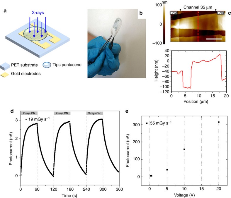
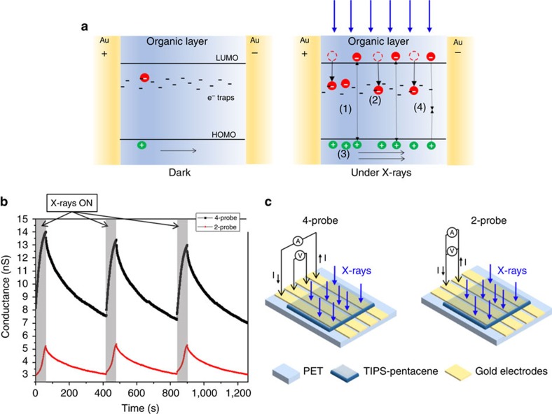
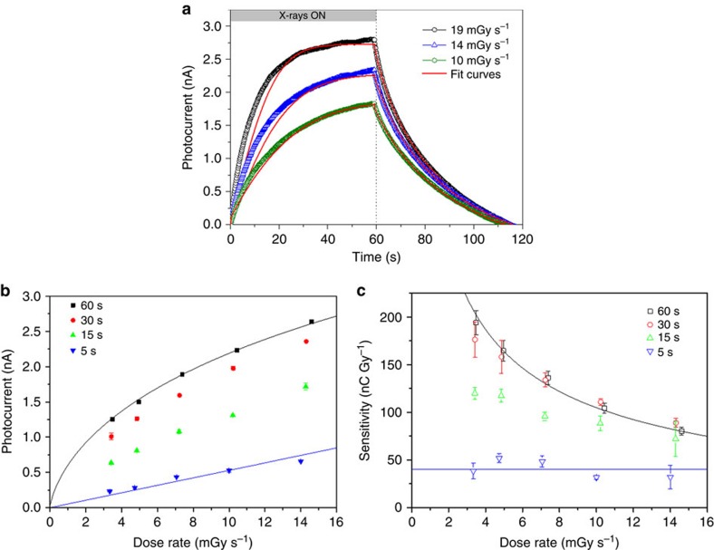
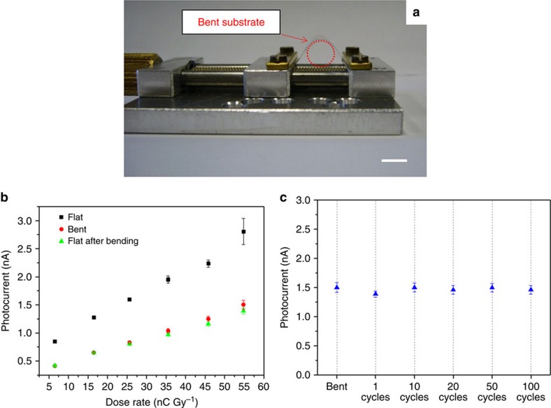
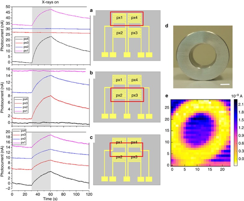
The application of organic electronic materials for the detection of ionizing radiations is very appealing thanks to their mechanical flexibility, low-cost and simple processing in comparison to their inorganic counterpart. In this work we investigate the direct X-ray photoconversion process in organic thin film photoconductors. The devices are realized by drop casting solution-processed bis-(triisopropylsilylethynyl)pentacene (TIPS-pentacene) onto flexible plastic substrates patterned with metal electrodes; they exhibit a strong sensitivity to X-rays despite the low X-ray photon absorption typical of low-Z organic materials. We propose a model, based on the accumulation of photogenerated charges and photoconductive gain, able to describe the magnitude as well as the dynamics of the X-ray-induced photocurrent. This finding allows us to fabricate and test a flexible 2 × 2 pixelated X-ray detector operating at 0.2 V, with gain and sensitivity up to 4.7 × 10⁴ and 77,000 nC mGy-1 cm-3, respectively.


Figures

Figure 1
Figure 1. Flexible organic X-ray photodetectors based on TIPS-pentacene thin films.
(a) Schematic of the device structure. The organic active layer is drop-casted onto gold electrodes pre-deposited on flexible PET substrate in an interdigitated configuration. (b) Image showing the flexibility of the structure. (c) AFM micrograph (top) and height profile (bottom) of the TIPS-pentacene crystal domains within the channel region (white scale bar: 10 μm). (d) X-ray-induced photocurrent signal recorded at a bias voltage of 0.2 V, upon three on/off switching cycles of a monochromatic synchrotron X-ray beam at 17 keV. (e) Photocurrent signal at different bias voltages recorded under an X-ray beam by a Mo-target X-ray tube with a dose rate of 55 mGy s−1.
Figure 2
Figure 2. Charge accumulation in the X-ray photo-response of organic detectors.
(a) Schematic of the process of modulation of the conductivity induced by X-rays exposure of TIPS-pentacene thin films: (left) in dark the conductivity is due to the intrinsic carriers; (right) under X-ray irradiation: (1) additional electrons and holes are generated; after generation holes drift along the electric field until they reach the collecting electrode while (2) electrons remain trapped in deep trap states within the organic material. (3) To guarantee charge neutrality, holes are continuously emitted from the injecting electrode. As a consequence, for each electron-hole pair created, more than one hole contributes to the photocurrent leading to a photoconductive gain effect. (4) Recombination process takes place, counterbalancing the charge photogeneration in the steady-state. (b) Plots of the 4-probe (black squares) and 2-probe (red circles) measurements upon three switching on and off the X-ray beam (the grey regions in the plot indicate when the device is under irradiation). The X-ray source is a Mo-target tube with 35 kV of accelerating voltage. (c) Schematic of the electrode configuration used for the 4-probe (left) and the 2-probe (right) measurements reported in b.
Figure 3
Figure 3. Dynamics of X-ray response and consequences on detector operation.
(a) Experimental and simulated curves of the dynamic response of the detector for three different dose rates of the radiation. The experimental data refer to 60 s of exposure of the device (W=48 mm, L=30 μm, bias 0.2 V) to a synchrotron 17 keV X-ray beam, with a bias of 0.2 V. (b) Photocurrent versus Dose rate plot (scattered points) recorded for different exposure times of the device to a synchrotron monochromatic X-ray beam at 17 keV and biasing the device at 0.2 V. (c) Sensitivity values, founded differentiating the photocurrent data in function of dose rate (reported in a), versus dose rate for different time exposures of the device to the radiation. Solid lines in (ac) represent fits to the data according to the analytical model described in the text. The error bars in c are calculated by means of error propagation theory from errors of experimental data reported in b.
Figure 4
Figure 4. Assessment of the mechanical reliability of the system.
(a) Experimental set-up used for the characterization of the detector during bending (scale bar: 1 cm). (b) Photocurrent as a function of dose rate of a device measured before bending (black solid squares), during bending with a bending radius of 0.3 cm (red solid circles) and after bending (green solid triangles). (c) Photocurrent of a device measured under bending and in flat-substrate condition after the 1, 10, 20, 50 and 100 bending cycles, at the same bending radius R=0.3 cm. The device (W=26 mm; L=30 μm), biased at 0.5 V, is irradiated under an X-ray beam provided by a Mo-tube with 35 kV of accelerating voltage and a dose rate of 55 mGy s−1.
Figure 5
Figure 5. 2 × 2 pixel matrix organic detector.
Left: X-ray-induced current signals versus time, recorded by selectively irradiating the pixels of a 2 × 2 detector matrix. The radiation source employed is a monochromatic synchrotron X-ray beam at 17 keV with a dose rate of 28.5 mGy s−1. The pixels (with W=48 mm and L=30 μm) were all biased at 0.2 V. Note that the baseline of the four photocurrent signals are shifted in y axis for clarity. Centre: a sketch of the device is reported, with the red box indicating the region of the matrix under irradiation. In particular: in a only pixels 1 and 4 are irradiated, in b only pixels 2 and 3 are irradiated, in c all the pixels are irradiated. Right: photograph (d) and corresponding X-ray image by a single pixel device (e) of an aluminium annular ring; the scale bar is 5 mm.

Similar articles

Cited by

References

    1. Owens A. & Peacock A. Compound semiconductor radiation detectors. Nucl. Instrum. Methods Phys. Res. Sect. Accel. Spectrometers Detect. Assoc. Equip. 531, 18–37 (2004).
    1. Zygmanski P., Abkai C., Han Z., Shulevich Y. & Menichelli D. Low-cost flexible thin-film detector for medical dosimetry applications. J. Appl. Clin. Med. Phys. 15, 4454 (2014). - PMC - PubMed
    1. Wang K., Chen F., Belev G., Kasap S. & Karim K. S. Lateral metal-semiconductor-metal photodetectors based on amorphous selenium. Appl. Phys. Lett. 95, 013505 (2009).
    1. Bruzzi M. et al.. Zero-bias operation of polycrystalline chemically vapour deposited diamond films for Intensity Modulated Radiation Therapy. Diam. Relat. Mater. 20, 84–92 (2011).
    1. Basiricò L., Cosseddu P., Fraboni B. & Bonfiglio A. Inkjet printing of transparent, flexible, organic transistors. Thin Solid Films 520, 1291–1294 (2011).

Publication types