. 2016 Oct 7:6:34861.
doi: 10.1038/srep34861.

Large gap Quantum Spin Hall Insulators of Hexagonal III-Bi monolayer

Affiliations

Large gap Quantum Spin Hall Insulators of Hexagonal III-Bi monolayer

Qunqun Liu et al. Sci Rep. .

Abstract

In the present work, we demonstrate that both GaBi3 and InBi3 monolayers are Quantum Spin Hall insulators. Here, the electronic band structures and edge states of the two novel monolayers are systematically investigated by first principle calculation. Our analysis of the band inversion and Z2 number demonstrate that both GaBi3 and InBi3 are promising 2D TIs with large gaps of 283meV and 247meV, respectively. Taking GaBi3 as example, it is illustrated that the edge states are impacted by SOC and finite size effect. In addition, it is found that the compression and tension totally affect differently on the edge states. Finally, the electron velocity is studied in detail, which is highly important in the manufacturing of spintronics device.


Figures

Figure 1
Figure 1
(a) Geometric structure of XBi3 monolayer. The purple balls represent Bi atoms and the green balls represent X (X = Ga, In, Tl) atoms. (b) First Brillioun zone of XBi3. (c,d) Top and side view of geometric structure of XBi3 primitive cell. (e) Phonon spectrum of GaBi3 and InBi3 (TlBi3 is omitted for its metallic character).
Figure 2
Figure 2. Upper part: The electronic bulk band structures of GaBi3, InBi3, TlBi3.
The blue lines and red lines represent the band structures without and with SOC, respectively. The horizontal purple dashed line indicates the Fermi level. Lower part: The evolution from atomic p-orbit of Ga and Bi to VBM and CBM at Γ point for XBi3, fermi level (Ef) is indicated by the red dashed line. The parities of the states at Γ point are denoted by + and −.
Figure 3
Figure 3
(a) The geometric structure of XBi3(X = Ga, In) nanoribbon. (b,c) Electronic band structures of GaBi3 and InBi3 nanoribbon. The blue or green shadow part represent the bulk energy spectrum, the red line represent the edge states. The widths are 9.8 nm and 12.0 nm for GaBi3 and InBi3 respectively.
Figure 4
Figure 4
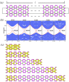
(a) Nanoribbon of GaBi3 (b) Electronic band structures for the GaBi3 zigzag nanoribbons of 2.4 nm, 3.6 nm. 6.4 nm, 7.9 nm and 9.8 nm, respectively (c) Real space charge density distribution of the edge states at Γ points.
Figure 5
Figure 5
GaBi3 monolayers under strain from −8% to +8% for (a) bulk energy spectrums according to strain (b) edge states according to strain. (c) The variation of the bulk direct gap Eg(Γ) at the Γ point and the indirect band gap Eg as a function of external strain. (d) Variation of the ribbon edge gap as a function of external strain. (e) Electron velocity near Fermi level at Γ point with the strain from −8% to 2%.

References

    1. Kane C. L. & Mele E. J. Quantum Spin Hall Effect in Graphene. Phys. Rev. Lett. 95, 226801 (2005). - PubMed
    1. Kane C. L. & Mele E. J. Z2 topological order and the quantum spin Hall effect. Phys. Rev. Lett. 95, 146802 (2005). - PubMed
    1. Bernevig B. A. & Zhang S. C. Quantum spin Hall effect. Phys. Rev. Lett. 96, 106802 (2006). - PubMed
    1. Bernevig B. A., Hughes T. L. & Zhang S. C. Quantum Spin Hall Effect and Topological Phase Transition in HgTe Quantum Wells. Science 314, 1757–1761 (2006). - PubMed
    1. Fu L., Kane C. L. & Mele E. J. Topological Insulators in Three Dimensions. Phys. Rev. Lett. 98, 106803 (2007). - PubMed

Publication types

LinkOut - more resources