

Effective suppression of efficiency droop in GaN-based light-emitting diodes: role of significant reduction of carrier density and built-in field
- PMID: 27756916
- PMCID: PMC5069459
- DOI: 10.1038/srep34586
Effective suppression of efficiency droop in GaN-based light-emitting diodes: role of significant reduction of carrier density and built-in field
Abstract
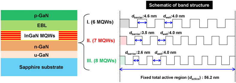
A critical issue in GaN-based high power light-emitting diodes (LEDs) is how to suppress the efficiency droop problem occurred at high current injection while improving overall quantum efficiency, especially in conventional c-plane InGaN/GaN quantum well (QW), without using complicated bandgap engineering or unconventional materials and structures. Although increasing thickness of each QW may decrease carrier density in QWs, formation of additional strain and defects as well as increased built-in field effect due to enlarged QW thickness are unavoidable. Here, we propose a facile and effective method for not only reducing efficiency droop but also improving quantum efficiency by utilizing c-plane InGaN/GaN QWs having thinner barriers and increased QW number while keeping the same single well thickness and total active layer thickness. As the barrier thickness decreases and the QW number increases, both internal electric field and carrier density within QWs are simultaneously reduced without degradation of material quality. Furthermore, we found overall improved efficiency and reduced efficiency droop, which was attributed to the decrease of the built-in field and to less influence by non-radiative recombination processes at high carrier density. This simple and effective approach can be extended further for high power ultraviolet, green, and red LEDs.
Figures


Similar articles
-
Reducing the efficiency droop by lateral carrier confinement in InGaN/GaN quantum-well nanorods.Opt Express. 2014 May 5;22 Suppl 3:A790-9. doi: 10.1364/OE.22.00A790. Opt Express. 2014. PMID: 24922386
-
Nonradiative recombination--critical in choosing quantum well number for InGaN/GaN light-emitting diodes.Opt Express. 2015 Feb 9;23(3):A34-42. doi: 10.1364/OE.23.000A34. Opt Express. 2015. PMID: 25836251
-
Thermal and efficiency droop in InGaN/GaN light-emitting diodes: decoupling multiphysics effects using temperature-dependent RF measurements.Sci Rep. 2019 Dec 27;9(1):19921. doi: 10.1038/s41598-019-56390-2. Sci Rep. 2019. PMID: 31882667 Free PMC article.
-
A Review on Experimental Measurements for Understanding Efficiency Droop in InGaN-Based Light-Emitting Diodes.Materials (Basel). 2017 Oct 26;10(11):1233. doi: 10.3390/ma10111233. Materials (Basel). 2017. PMID: 29072611 Free PMC article. Review.
-
Factors Affecting Surface Plasmon Coupling of Quantum Wells in Nitride-Based LEDs: A Review of the Recent Advances.Nanomaterials (Basel). 2021 Apr 27;11(5):1132. doi: 10.3390/nano11051132. Nanomaterials (Basel). 2021. PMID: 33925717 Free PMC article. Review.
Cited by
-
Optimal Silicon Doping Layers of Quantum Barriers in the Growth Sequence Forming Soft Confinement Potential of Eight-Period In0.2Ga0.8N/GaN Quantum Wells of Blue LEDs.Nanoscale Res Lett. 2017 Nov 9;12(1):591. doi: 10.1186/s11671-017-2359-3. Nanoscale Res Lett. 2017. PMID: 29124372 Free PMC article.
-
Electrically driven, highly efficient three-dimensional GaN-based light emitting diodes fabricated by self-aligned twofold epitaxial lateral overgrowth.Sci Rep. 2017 Aug 29;7(1):9663. doi: 10.1038/s41598-017-10086-7. Sci Rep. 2017. PMID: 28852044 Free PMC article.
-
A comparative study of efficiency droop and internal electric field for InGaN blue lighting-emitting diodes on silicon and sapphire substrates.Sci Rep. 2017 Apr 12;7:44814. doi: 10.1038/srep44814. Sci Rep. 2017. PMID: 28401941 Free PMC article.
-
Thermophysical Characterization of Efficiency Droop in GaN-Based Light-Emitting Diodes.Nanomaterials (Basel). 2021 May 30;11(6):1449. doi: 10.3390/nano11061449. Nanomaterials (Basel). 2021. PMID: 34070771 Free PMC article.
-
Ultra-low-current driven InGaN blue micro light-emitting diodes for electrically efficient and self-heating relaxed microdisplay.Nat Commun. 2023 Mar 17;14(1):1386. doi: 10.1038/s41467-023-36773-w. Nat Commun. 2023. PMID: 36932091 Free PMC article.
References
-
- Piprek J. Efficiency droop in nitride-based light-emitting diodes. Phys. Status Solidi A 207, 2217 (2010).
-
- Mayarrd D. S. et al.. Asymmetry of carrier transport leading to efficiency droop in InGaN-based light emitting diode. Appl. Phys. Lett. 99, 251115 (2010).
-
- Zhu D. et al.. Enhanced electron capture and symmetrized carrier distribution in InGaN light emitting diodes having tailored barrier doping. Appl. Phys. Lett. 96, 121110 (2010).
-
- Shen Y. C. et al.. Auger recombination in InGaN measured by photoluminescence. Appl. Phys. Lett. 91, 141101 (2007).
-
- Efremov A. A. et al.. Effect of the joule heating on the quantum efficiency and choice of thermal conditions for high-power blue InGaN/GaN LEDs. Semiconductors 40, 605 (2006).
Publication types
LinkOut - more resources
Full Text Sources
Other Literature Sources
Research Materials
