. 2016 Oct 18;113(42):11682-11687.
doi: 10.1073/pnas.1605269113.

Ultrathin, transferred layers of thermally grown silicon dioxide as biofluid barriers for biointegrated flexible electronic systems

Affiliations

Ultrathin, transferred layers of thermally grown silicon dioxide as biofluid barriers for biointegrated flexible electronic systems

Hui Fang et al. Proc Natl Acad Sci U S A. .

Abstract

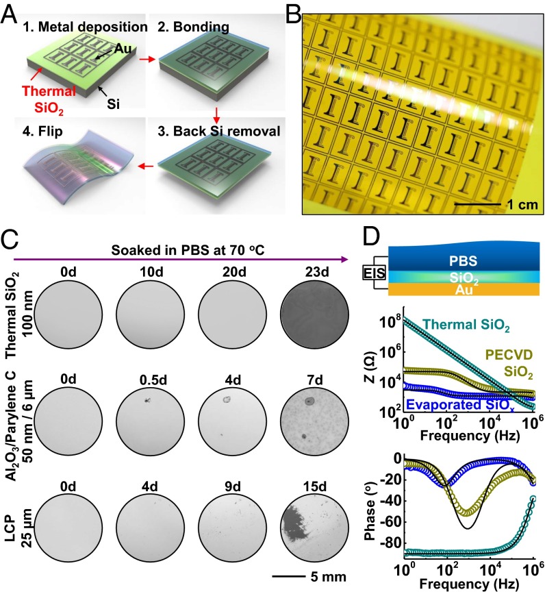
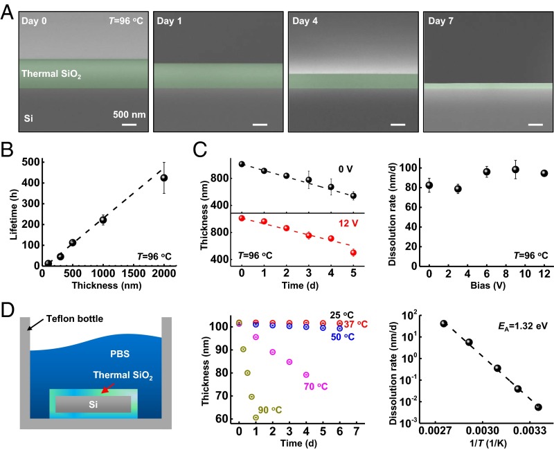
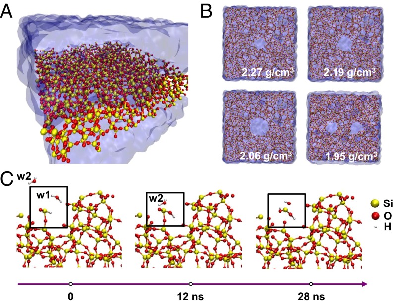
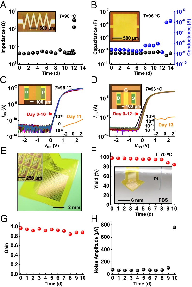
Materials that can serve as long-lived barriers to biofluids are essential to the development of any type of chronic electronic implant. Devices such as cardiac pacemakers and cochlear implants use bulk metal or ceramic packages as hermetic enclosures for the electronics. Emerging classes of flexible, biointegrated electronic systems demand similar levels of isolation from biofluids but with thin, compliant films that can simultaneously serve as biointerfaces for sensing and/or actuation while in contact with the soft, curved, and moving surfaces of target organs. This paper introduces a solution to this materials challenge that combines (i) ultrathin, pristine layers of silicon dioxide (SiO2) thermally grown on device-grade silicon wafers, and (ii) processing schemes that allow integration of these materials onto flexible electronic platforms. Accelerated lifetime tests suggest robust barrier characteristics on timescales that approach 70 y, in layers that are sufficiently thin (less than 1 μm) to avoid significant compromises in mechanical flexibility or in electrical interface fidelity. Detailed studies of temperature- and thickness-dependent electrical and physical properties reveal the key characteristics. Molecular simulations highlight essential aspects of the chemistry that governs interactions between the SiO2 and surrounding water. Examples of use with passive and active components in high-performance flexible electronic devices suggest broad utility in advanced chronic implants.

Keywords: chronic implant; reactive molecular simulation; thermal silicon dioxide; thin-film encapsulation; transfer printing.


Conflict of interest statement

The authors declare no conflict of interest.

Figures

Fig. 1.
Fig. 1.
Materials and integration strategies for use of ultrathin layers of SiO2 thermally grown on device-grade silicon wafers, as water barriers in flexible electronics. (A) Schematic illustration of schemes for exploiting layers of thermal SiO2 for encapsulation in test structures: (1) electron beam evaporation, photolithography, and etching of Mg to form “I”-shape patterns as test structures on SiO2 thermally grown on a silicon wafer; (2) pressure bonding the top surface to a glass substrate that supports a thin film of polyimide (Kapton; 25 µm); (3) removal of the silicon wafer from back side by dry etching; (4) release of the final flexible test structure from the glass substrate. (B) Optical image of a sample produced in this manner, with a ∼100-nm-thick layer of thermal SiO2 on its top surface. (C) Sequential images of Mg encapsulated by layers of thermal SiO2 and Al2O3/Parylene C and a bulk film of liquid crystal polymer (LCP) soaked in PBS solution at 70 °C. (D) EIS and modeling results for layers of SiO2 grown by thermal oxidation and deposited by PECVD and electron beam evaporation.
Fig. 2.
Fig. 2.
Failure mechanisms associated with thermal SiO2 encapsulation layers. (A) SEM images showing decreases in the thickness of a 1,000-nm-thick layer of thermal SiO2 as a result of soaking in PBS at 96 °C. (B) Time before the leakage current reaches more than 100 nA, for thermal SiO2 measured in an electrical leakage test (described in SI Appendix, Fig. S4). (C) Thickness changes associated with a 1,000-nm-thick layer of thermal SiO2 without DC bias and with 12-V bias (Left), and extracted dissolution rate for voltages of 0, 3, 6, 9, and 12 V (Right). (D) Thermal SiO2 on the surfaces and edges of a piece of Si in PBS solution (Left) allowed measurements of changes in thickness at different temperatures (Center). The results indicate a linear relationship between the dissolution rate and 1/T (Right).
Fig. 3.
Fig. 3.
Reactive molecular dynamics (RMD) simulations of hydrolysis of defective layers of SiO2. (A) Perspective snapshot of the SiO2 slab in water. (B) Top-view representation of four different oxide densities of the SiO2 slab in water. (C) Simulation snapshots of hydrolysis reactions that lead to the dissociation of one molecule of SiO2 from the structure.
Fig. 4.
Fig. 4.
Demonstration of electronic devices and flexible electronic systems encapsulated with thermal SiO2. (A–D) Results of soak tests of resistors, capacitors, diodes, and n-type metal–oxide–semiconductor transistors with optical images (Insets). Tests in PBS solutions at 96 °C indicate that failure occurs at day 12 for all devices. (E) A photograph of a platform of active multiplexed flexible electronics with double-sided thermal SiO2 encapsulation in a slightly bent configuration. The Inset presents a magnified view of the sensing sites, each of which consists of one sensing transistor and one multiplex transistor connected in series. (F–H) Accelerating soak test with in vitro measurement of electrical performance including yield (Y/Y0, defined as the number of working sensing sites divided by the total number of sites), gain (the ideal gain is 1), and mean noise rms. The results indicate device stability throughout 9 d in 70 °C PBS. The Inset in F presents a photograph of an active multiplex device fully immersed in PBS.

References

    1. Kim D-H, et al. Epidermal electronics. Science. 2011;333(6044):838–843. - PubMed
    1. Lipomi DJ, et al. Skin-like pressure and strain sensors based on transparent elastic films of carbon nanotubes. Nat Nanotechnol. 2011;6(12):788–792. - PubMed
    1. Xu S, et al. Soft microfluidic assemblies of sensors, circuits, and radios for the skin. Science. 2014;344(6179):70–74. - PubMed
    1. Gao W, et al. Fully integrated wearable sensor arrays for multiplexed in situ perspiration analysis. Nature. 2016;529(7587):509–514. - PMC - PubMed
    1. Wu W, et al. Piezoelectricity of single-atomic-layer MoS2 for energy conversion and piezotronics. Nature. 2014;514(7523):470–474. - PubMed

Publication types

Substances