. 2016 Feb 4;3(8):1500343.
doi: 10.1002/advs.201500343. eCollection 2016 Aug.

Progress and Challenges in Transfer of Large-Area Graphene Films

Affiliations

Progress and Challenges in Transfer of Large-Area Graphene Films

Yi Chen et al. Adv Sci (Weinh). .

Abstract

Graphene, the thinnest, strongest, and stiffest material with exceptional thermal conductivity and electron mobility, has increasingly received world-wide attention in the past few years. These unique properties may lead to novel or improved technologies to address the pressing global challenges in many applications including transparent conducting electrodes, field effect transistors, flexible touch screen, single-molecule gas detection, desalination, DNA sequencing, osmotic energy production, etc. To realize these applications, it is necessary to transfer graphene films from growth substrate to target substrate with large-area, clean, and low defect surface, which are crucial to the performances of large-area graphene devices. This critical review assesses the recent development in transferring large-area graphene grown on Fe, Ru, Co, Ir, Ni, Pt, Au, Cu, and some nonmetal substrates by using various synthesized methods. Among them, the transfers of the most attention kinds of graphene synthesized on Cu and SiC substrates are discussed emphatically. The advances and the main challenges of each wet and dry transfer method for obtaining the transferred graphene film with large-area, clean, and low defect surface are also reviewed. Finally, the article concludes the most promising methods and the further prospects of graphene transfer.

Keywords: challenges; dry transfer methods; graphene films; promising methods; wet transfer methods.


Figures

Figure 1
Figure 1
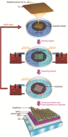
Illustration of the process of PMMA‐mediated nanotransfer printing technique. Reproduced with permission.37 2008, American Chemical Society.
Figure 2
Figure 2
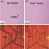
Optical micrographs of graphene transferred on the SiO2/Si wafers by a) the traditional method and b) second coated PMMA method. Optical images of large folds c) before and d) after baking the stack at 150 °C. a,b) Reproduced with permission.41 2009, American Chemical Society. c,d) Reproduced with permission.42 2011, American Chemical Society.
Figure 3
Figure 3
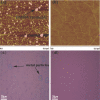
The AFM images of the graphene surface after removal of PMMA via different routes. a) The traditional method: PMMA was treated by acetone for 2 h. b) The improved method: acetone vapor, 2 min acetone immersion, and 3 h of annealing. The typical high‐magnification optical images of the graphene film c) before and d) after the “RCA” process. a,b) Reproduced with permission.49 2012, American Chemical Society. c,d) Reproduced with permission.42 2011, American Chemical Society.
Figure 4
Figure 4
Schematic diagram of the “Polymer‐free” transfer method. Reproduced with permission.54 2014, American Chemical Society.
Figure 5
Figure 5
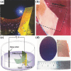
a) Illustration of the “bubble” transfer method. b) Illustration of the “bubble‐free” transfer method. c) Schematic diagram of the electrochemical exfoliation method. d) Graphene was transferred onto a 4 inch wafer by the “bubble” transfer method. a,c,d) Reproduced with permission.59 2011, American Chemical Society. b) Reproduced with permission.62
Figure 6
Figure 6
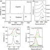
a) Raman spectrum at 514 nm for bulk graphite and graphene. b) Raman spectrum of graphene at 514 nm with the number of layers. c) D peak at the edge of bulk graphite and single layer graphene. d) The four components of the 2D peak in two layer graphene at 514 and 633 nm. Reproduced with permission.65 2006, American Physical Society.
Figure 7
Figure 7
The schematic diagram of the two kinds of “roll‐to‐roll” transfer methods. a) Reproduced with permission.28 2010, Nature Publishing Group. b) Reproduced with permission.77 2010, Elsevier.
Figure 8
Figure 8
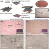
a) Schematic diagram of graphene transferred by “roll‐to‐roll” and hot pressing. b,c) Optical and c,d) SEM images showing the surface morphologies of the graphene films transferred onto SiO2/Si substrates by “roll‐to‐roll” and hot pressing respectively. Reproduced with permission.72 2012, American Chemical Society.
Figure 9
Figure 9
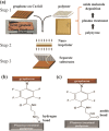
a) Schematic diagram of the dry transfer methods. b) Hydrogen bond and c) covalent bond formed between the TFPA and the polystyrene surface. Reproduced with permission.78 2012, American Chemical Society.
Figure 10
Figure 10
a,b) Schematic diagram of the face‐to‐face method for transferring graphene mediated by capillary bridges. c) Photograph of the transferred graphene on an 8 in. wafer and 4 in. wafer. d) Raman spectrum of graphene transferred by face‐to‐face transfer (red), float transfer onto SiO2/Si substrates (blue) and graphene on Cu film before transfer (green). Reproduced with permission.36 2013, Nature Publishing Group.
Figure 11
Figure 11
a–e) Schematic diagram of the method to transfer epitaxial graphene grown on SiC substrate. f) Raman spectrum of graphene grown SiC, the width of the 2D peak (72.6 cm–1) suggests multilayer graphene. The D peak is not observed in this sample. g) Raman spectrum of the transferred graphene, the D peak is observed in this sample, which suggests a high density of defects of the graphene. a–e) Reproduced with permission.82 Copyright 2009, American Institute of Physics. f,g) Reproduced with permission.83 2010, American Chemical Society.

References

    1. Novoselov K. S., Geim A. K., Morozov S. V., Jiang D., Zhang Y., Dubonos S. V., Grigorieva I. V., Firsov A. A., Science 2004, 306, 666. - PubMed
    1. Lee C., Wei X., Kysar J. W., Hone J., Science 2008, 321, 385. - PubMed
    1. Chen J. H., Jang C., Ishigami M., Nat. Nanotechnol 2008, 3, 206. - PubMed
    1. Ghosh S., Nika D. L., Pokatilov E. P., Balandin A. A., New J. Phys. 2009, 11, 095012.
    1. Xia F., Farmer D. B., Lin Y. M., Avouris P., Nano Lett. 2010, 10, 715. - PubMed