. 2016 Feb 18;3(8):1500362.
doi: 10.1002/advs.201500362. eCollection 2016 Aug.

Interfacial Materials for Organic Solar Cells: Recent Advances and Perspectives

Affiliations

Interfacial Materials for Organic Solar Cells: Recent Advances and Perspectives

Zhigang Yin et al. Adv Sci (Weinh). .

Abstract

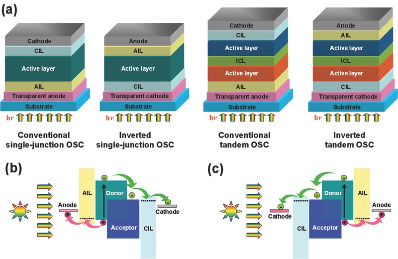
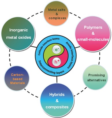
Organic solar cells (OSCs) have shown great promise as low-cost photovoltaic devices for solar energy conversion over the past decade. Interfacial engineering provides a powerful strategy to enhance efficiency and stability of OSCs. With the rapid advances of interface layer materials and active layer materials, power conversion efficiencies (PCEs) of both single-junction and tandem OSCs have exceeded a landmark value of 10%. This review summarizes the latest advances in interfacial layers for single-junction and tandem OSCs. Electron or hole transporting materials, including metal oxides, polymers/small-molecules, metals and metal salts/complexes, carbon-based materials, organic-inorganic hybrids/composites, and other emerging materials, are systemically presented as cathode and anode interface layers for high performance OSCs. Meanwhile, incorporating these electron-transporting and hole-transporting layer materials as building blocks, a variety of interconnecting layers for conventional or inverted tandem OSCs are comprehensively discussed, along with their functions to bridge the difference between adjacent subcells. By analyzing the structure-property relationships of various interfacial materials, the important design rules for such materials towards high efficiency and stable OSCs are highlighted. Finally, we present a brief summary as well as some perspectives to help researchers understand the current challenges and opportunities in this emerging area of research.

Keywords: energy conversion; interface engineering; interlayers; organic solar cells; semiconductors.


Figures

Figure 1
Figure 1
a) Schematic device architectures of conventional and inverted single‐junction/tandem OSCs. AIL: anode interface layer; CIL: cathode interface layer; ICL: interconnecting layer. Schematic illustration of the energy level diagrams and the main charge‐transporting processes in b) conventional and c) inverted OSCs.
Figure 2
Figure 2
Schematic illustration of material categories for cathode interface layers, anode interface layers, and interconnecting layers used in OSCs.
Figure 3
Figure 3
a) Molecular structures of PIFTBT8 and PC71BM, and a schematic device with the ZnO CIL. b) Current density‐voltage (J−V) characteristics under AM 1.5G irradiation (100 mW cm−2), and c) Device stability of the inverted OSCs with ZnO CILs derived from controlled precursor solutions. Reproduced with permission.48 Copyright 2013, American Chemical Society. d) Average performance parameters of devices with ZnO CILs derived from ZnAc (red circles), deZn (blue triangles), PA‐modified ZnAc (green squares), and PA‐modified deZn (gray diamonds): V OC, FF, J SC, and PCE, all as a function of time exposed to the degradation solar simulator. Reproduced with permission.71 Copyright 2015, Royal Society of Chemistry.
Figure 4
Figure 4
a) Schematic illustration of a preparation process for OSCs containing dual‐sided nanoimprinted DNAs. b) Total transmittance and haze values of ZnO/ITO glasses without and with DNA‐patterns. The inset depicts the optical measurement configuration using an integrating sphere. c) JV and d) J phV eff characteristics for the reference and patterned OSCs under AM 1.5G illumination. Reproduced with permission.10
Figure 5
Figure 5
a) A schematic device structure based on the ZMO CIL. b) Energy levels of the components in the OSCs with various ZMO as the CIL. c) Optical absorption spectra of ZMO films. The inset shows an increase in the bandgap of ZMO films. d) Device stability of three types of devices: the best ZMO CIL‐based inverted OSC (▪), the PEDOT:PSS‐based conventional OSC (●), and the inverted OSC without a CIL (▴).Reproduced with permission.57
Figure 6
Figure 6
Molecular structures of some representative polymers and small‐molecules for CILs.
Figure 7
Figure 7
Thickness dependence of device performance on the C60‐SB CIL (error represents ±1 standard deviation over eight devices). Reproduced with permission.164
Figure 8
Figure 8
a) Schematic illustration of the inverted OSC with a hybrid PEG–TiOx CIL. b) Molecule structures of PDTTBT‐3, PTB7, PTB7‐Th and PC71BM. c) Energy levels of each component used in the OSCs. d) WFs of ITO, TiOx and PEG–TiOx films determined by a Kelvin probe technique. Improved device performance of different polymer‐based OSCs using the PEG–TiOx CIL: e) J–V characteristics under AM 1.5G irradiation (100 mW cm−2), and f) Device stability of the OSCs. Reproduced with permission.27 Copyright 2015, Springer.
Figure 9
Figure 9
a) Schematic device structure based on the hybrid CIL of ZnO:PBI‐H. b) IV curves for the device with ITO/ZnO:PBI‐H (90 nm)/Al in the dark and under AM 1.5G illumination. The inset is the chemical structure of PBI‐H. Reproduced with permission.177 Copyright 2015, American Chemical Society.
Figure 10
Figure 10
a) A schematic conventional OSC based on the polyoxometalate (POM) CIL. b) Molecular structures of Keggin and Dawson POMs used in this study. c) Molecular orbital diagrams of various POMs. d) J–V characteristics under AM 1.5G illumination of the OSCs using various CILs. Reproduced with permission.190 Copyright 2015, American Chemical Society.
Figure 11
Figure 11
a) A schematic OSC using metal NPs‐doped PEDOT:PSS as an AIL. b) The scattering power and absorption power of the 45 nm Au NPs and 45 nm@10 nm Au@Ag NCs. The scattering enhancement of the Au@Ag NCs compared to that of the Au NPs is plotted as a green line. c) J–V curves of a control PEDOT:PSS device and the best plasmonic PTB7:PC71BM OSCs with the Au NPs and Au@Ag NCs embedded. The inset graph includes TEM images (left, scale bar: 20 nm), scattered electric field |E| 2 distributions (middle), and scattering images (right) of the Au NPs and Au@Ag NCs. Reproduced with permission.46 Copyright 2014, American Chemical Society.
Figure 12
Figure 12
a) Schematic synthesis of p‐PFPs by oxidative treatments of n‐type PFP with persulfate salts. b) Illustration of p‐PFP configurations with varying degree of doping concentration (left) on metal electrodes and their plausible dipole formation (right) at interfaces between the electrode and n‐type PFP (right upper image) or p‐PFP (right lower image); sky blue: π‐conjugated backbone, red (−): alkyl side chain bearing a sulfonate functional group, blue (+): oxidized π‐conjugated backbone, yellow (+): a sodium counter ion, red dashed line: electrostatic interaction between sulfonate ion and hydrogen. The red and blue arrows represent the dipole direction of the ion‐induced dipoles (μ ID) and polaron‐induced dipoles (μ PD), respectively. c) Ultraviolet photoelectron spectroscopy spectra of the ITO with and without p‐PFPs. The inset displays the effective WFs of the ITO (open circle) coated with thin AILs of PFP (orange), p‐PFP‐WD (olive), p‐PFP‐MD (blue), and p‐PFP‐HD (red). d) J–V characteristics of the OSCs using different AILs. Reproduced with permission.266
Figure 13
Figure 13
a) A schemetic tandem OSC with an e‐h‐type ICL of CPE1/CPE2/m‐PEDOT:PSS (left), the proposed scenario of self‐assembly bilayer CPE1/CPE2 (middle), and the schematic energy diagram (right) of the WF change due to the presence of CPEs between the front and back subcells. Reproduced with permission.306 Copyright 2013, Macmillan Publishers Limited. b) A schemetic tandem device with an ICL of ZnO/CPE (left), chemical structures of two HTLs (middle), and the energy diagram (right) of individual layers used in the tandem OSCs. Reproduced with permission.30
Figure 14
Figure 14
a) The triple tandem OSC using a h‐c‐e‐type ICL of WO3/PEDOT:PSS/ZnO (left) and the relevant energy level diagram (right). LBG represents PDTP‐DFBT, and PTB represents PTB7‐Th. Reproduced with permission.29 b) The triple tandem device with a h‐e‐type ICL of n‐PEDOT:PSS/ZnO/C60‐SAM (left) and the corresponding energy level diagram (right). Reproduced with permission.31 Copyright 2015, Royal Society of Chemistry.
Figure 15
Figure 15
a) A schematic structure of flexible ITOSCs using the PEDOT/ZnO/Ba(OH)2 ICL. b) Schematic illustration of the interconnection lines in the organic tandem module (3 cells module). c) Photograph of one of the 9 substrates carrying two reference single tandem cells (center) and two pairs of tandem modules (left and right), with narrow (≈25 μm, left) and wide (≈325 μm, right) P2 line patterning. The insets present top views from an optical microscope showing the lines P1–P3. The wide P2 line was realized by laser hatching (scanning many single lines parallel to each other). d) J–V characteristics of the reference ITOSC and tandem modules with narrow (≈25 μm) and wide (≈325 μm) P2 lines under illumination. The inset shows the dark J–V characteristics. e) Normalized device characteristics of flexible tandem modules after 1000, 3000 and 5000 bending cycles. Reproduced with permission.330 Copyright 2014, Royal Society of Chemistry.

References

    1. Li G., Zhu R., Yang Y., Nat. Photon. 2012, 6, 153.
    1. Liu M., Johnston M. B., Snaith H. J., Nature 2013, 501, 395. - PubMed
    1. Mathew S., Yella A., Gao P., Humphry‐Baker R., Curchod B. F. E., Ashari‐Astani N., Tavernelli I., Rothlisberger U., Nazeeruddin M. K., Grätzel M., Nat. Chem. 2014, 6, 242. - PubMed
    1. Chuang C.‐H. M., Brown P. R., Bulović V., Bawendi M. G., Nat. Mater. 2014, 13, 796. - PMC - PubMed
    1. Günes S., Neugebauer H., Sariciftci N. S., Chem. Rev. 2007, 107, 1324. - PubMed