. 2016 Nov 21:6:37282.
doi: 10.1038/srep37282.

Realisation of magnetically and atomically abrupt half-metal/semiconductor interface: Co2FeSi0.5Al0.5/Ge(111)

Affiliations

Realisation of magnetically and atomically abrupt half-metal/semiconductor interface: Co2FeSi0.5Al0.5/Ge(111)

Zlatko Nedelkoski et al. Sci Rep. .

Abstract

Halfmetal-semiconductor interfaces are crucial for hybrid spintronic devices. Atomically sharp interfaces with high spin polarisation are required for efficient spin injection. In this work we show that thin film of half-metallic full Heusler alloy Co2FeSi0.5Al0.5 with uniform thickness and B2 ordering can form structurally abrupt interface with Ge(111). Atomic resolution energy dispersive X-ray spectroscopy reveals that there is a small outdiffusion of Ge into specific atomic planes of the Co2FeSi0.5Al0.5 film, limited to a very narrow 1 nm interface region. First-principles calculations show that this selective outdiffusion along the Fe-Si/Al atomic planes does not change the magnetic moment of the film up to the very interface. Polarized neutron reflectivity, x-ray reflectivity and aberration-corrected electron microscopy confirm that this interface is both magnetically and structurally abrupt. Finally, using first-principles calculations we show that this experimentally realised interface structure, terminated by Co-Ge bonds, preserves the high spin polarization at the Co2FeSi0.5Al0.5/Ge interface, hence can be used as a model to study spin injection from half-metals into semiconductors.


Figures

Figure 1
Figure 1
(a) Low magnification overview HAADF STEM image showing that the film is uniform with a thickness of ~18 nm. (b) SAED pattern from an area that includes both film and substrate, showing the single crystal nature of the grown film and the epitaxial relationship with the substrate. The motifs are labelled with the red dashed rectangle for the film and blue solid romb for the Ge substrate. (c) Simulated SAED diffraction pattern assuming twinned epitaxy with respect to the substrate which shows excellent agreement with the observations. The reflections labelled in red are from the film; in blue from the substrate. The reflections in grey appear due to double diffraction in the substrate.
Figure 2
Figure 2
(a) Overview HAADF STEM image along the [1-10] crystallographic direction, showing the abruptness of the CFAS/Ge interface. The white scale-bar corresponds to 0.7 nm. (b) Atomic resolution HAADF STEM image from the bulk-like film region showing the distinctive Co-(Fe-Si/Al) atomic planes repeat pattern along the [001] crystallographic direction characteristic for B2 ordered CFAS. The line profile along the white dashed rectangle is given in (d). (c) Atomic resolution HAADF STEM image from the interface region showing that the distinctive Co-(Fe-Si/Al) atomic planes repeat pattern along the [001] crystallographic direction is lost due to out-diffused Ge atoms from the substrate. The line profile along the white dashed rectangle is given in (e). The STEM images in (a,b) and (c) are obtained by rigid registration of a stack of images recorded in quick succession (resulting in high signal-to-noise and precision in the image). (g) Intensity signal coming from the Kα edge of Ge –blue curve, Co - red, Fe –yellow, Si –dark green, Al – light green; recorded during an EDXS linescan along the white solid line in (f).
Figure 3
Figure 3. EDXS chemical mapping across the interface.
(a) HAADF STEM image acquired simultaneously with the EDXS maps which serves as a reference image. The white scale-bar corresponds to 0.7 nm. (b) Ge Kα edge map showing the selective outdifussion of Ge across the reference interface plane (white dashed line). Yellow arrows are inserted as a guide to the eye. (c) Co Kα edge map showing the abrupt decrease of the Co signal across the interface. (d) Ge and Co overlaid map clearly showing the out-diffused Ge atoms in the Fe-Si/Al atomic planes which are in-between the Co(001) planes.
Figure 4
Figure 4. Atomic resolution HAADF STEM image of the interface showing that the CFAS film terminates on a Co(111) atomic plane.
This image is obtained by rigid registration of a stack of images of the same area recorded in quick succession (resulting in high signal-to-noise and precision in the image). The colour coding of the overlaid structural model is as follows: Ge –blue; Co –red; Fe-Si/Al –grey. The white scale-bar corresponds to 0.7 nm. The tilt angle of the Ge dumbbells from α = 37° in the bulk-like region increases to β = 51° for the interfacial Ge bilayer.
Figure 5
Figure 5
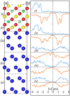
(a) Structural model of the CFAS/Ge interface viewed along the [1-10] crystallographic direction. (b) Spin-polarized PDOS for the regions labelled as (i–v) in (a). Spin-up PDOS are presented in the upper part of the plots, while spin-down in the lower part of the plots.
Figure 6
Figure 6. Magnetic profile across the CFAS/Ge interface obtained by PNR measurements.
Value zero on the distance axis corresponds to the interface.

References

    1. Kohn A., Lazarov V. K., Singh L. J., Barber Z. H. & Petford-Long A. K. The structure of sputter-deposited Co2MnSi thin films deposited on GaAs(001). J Appl Phys. 101, 023915 (2007).
    1. Kuerbanjiang B. et al.. The role of chemical structure on the magnetic and electronic properties of Co2FeAl0.5Si0.5/Si(111) interface. Appl Phys Lett. 108, 172412 (2016).
    1. Žutić I., Fabian J. & Das Sarma S. Spintronics: Fundamentals and applications. Rev Mod Phys. 76, 323 (2004).
    1. Jansen R. Silicon spintronics. Nat Mater. 11, 400 (2012). - PubMed
    1. Awschalom D. D. & Flatte M. E. Challenges for semiconductor spintronics. Nat Phys. 3, 153 (2007).

Publication types