Review
. 2009 Jan 13;10(1):013001.
doi: 10.1088/1468-6996/10/1/013001. eCollection 2009 Feb.

Hydrothermal growth of ZnO nanostructures

Affiliations
Review

Hydrothermal growth of ZnO nanostructures

Sunandan Baruah et al. Sci Technol Adv Mater. .

Abstract

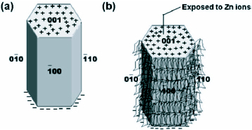
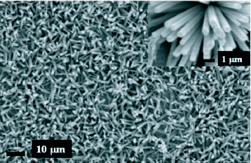
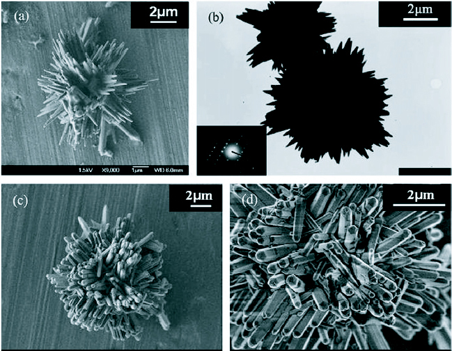
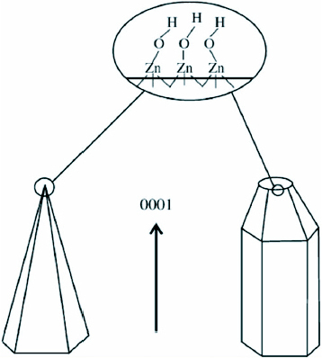
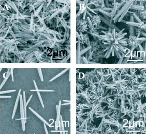
One-dimensional nanostructures exhibit interesting electronic and optical properties due to their low dimensionality leading to quantum confinement effects. ZnO has received lot of attention as a nanostructured material because of unique properties rendering it suitable for various applications. Amongst the different methods of synthesis of ZnO nanostructures, the hydrothermal method is attractive for its simplicity and environment friendly conditions. This review summarizes the conditions leading to the growth of different ZnO nanostructures using hydrothermal technique. Doping of ZnO nanostructures through hydrothermal method are also highlighted.

Keywords: ZnO; doping; hydrothermal; nanostructures; synthesis.


Figures

Figure 1
Figure 1
The wurtzite structure model of ZnO.
Figure 2
Figure 2
Growth morphologies of ZnO nanostructures with corresponding facets (reproduced with permission from [27] © 2004 IOP).
Figure 3
Figure 3
TEM images of the as synthesized ZnO nanoparticles using zinc nitrate hexahydrate in an autoclave at a temperature of 120 °C. (Reproduced with permission from [46] © 2006 Elsevier.)
Figure 4
Figure 4
Variation in particle size and yield of the ZnO nano powders with growth temperature and pH of the growth solution. Region A: heterogeneous solution; region B: homogeneous solution. (Reproduced with permission from [47] © 2000 Elsevier.)
Figure 5
Figure 5
Attachment of hexamine to the non polar facets of the zincite crystal allows the growth of the crystal in the (0001) direction. (a) hexagonal ZnO crystal (b) possible attachment of hexamine on to the non polar facets leaving the polar face exposed allowing further crystal growth along the c-direction. (Reproduced with permission from [57] © 2006 Springer.)
Figure 6
Figure 6
SEM image of ZnO nanorods grown using zinc nitrate and hexamine after seeding with ZnO nanoparticles. Inset: close up of the rods. (Reproduced with permission from authors [51].)
Figure 7
Figure 7
Images of ZnO homocentric bundles obtained in block copolymers systems: (a) SEM image: products in surfactant L64 (b) TEM image: products in L64. Inset: diffraction pattern. (c) and (d) SEM images: products in F68. (Reproduced with permission from [73] © 2007 Elsevier.)
Figure 8
Figure 8
Growth habits of hexagonal prism- and pyramid-like ZnO crystals. (Reproduced with permission from [73] © 2007 Elsevier.)
Figure 9
Figure 9
SEM images of the array of ZnO obelisk shaped nanorods grown on glass substrate. (Reproduced with permission from [75] © 2004 Elsevier.)
Figure 10
Figure 10
Illustration of the crystal structure of the obelisk shaped ZnO nanorods. (Reproduced with permission from [75] © 2004 Elsevier.)
Figure 11
Figure 11
SEM images of the ZnO nanostructures on Zn foil with condition mentioned in table 3: (a) A1 (b) A2 (c) A3 (d) A4. (Reproduced with permission from [78] © 2007 Elsevier.)
Figure 12
Figure 12
SEM images of the flower-like ZnO nanostructures at different magnifications. (Reproduced with permission from [79] © 2007 Elsevier.)
Figure 13
Figure 13
SEM images of ZnO nanoflowers synthesized using zinc chloride and ammonia. (Reproduced with permission from [80] © 2007 Elsevier.)
Figure 14
Figure 14
SEM images of as-synthesized ZnO micro and nanostructures prepared by CTAB-assisted hydrothermal growth at various temperatures (a) 120 °C (b) 150 °C and (c) 180 °C. Inset: magnified images. (Reproduced with permission from [81] © 2008 Elsevier.)
Figure 15
Figure 15
Schematic illustration explaining the growth of ZnO micro and nanostructures synthesized through CTAB-assisted hydrothermal process at different temperatures (a) 120 °C and (b) 150 °C and 180 °C. (Reproduced with permission from [81] © 2008 Elsevier.)
Figure 16
Figure 16
SEM images of the ZnO 3D nanostructures synthesized at different pH: (a) pH 9.0, (b) pH 9.5, (c) pH 10.0, (d) pH 10.5, (e) pH 11.0, (f) pH 11.5, (g) pH 11.8 and (h) magnified image of pH 11.8. (Reproduced with permission from [82] © 2008 Elsevier.)
Figure 17
Figure 17
TEM micrographs of the samples synthesized through microwave irradiation in aqueous solution of Zn(NO3)2 and pyridine at 90 °C for 10 min. (Reproduced with permission from [86] © 2007 Elsevier.)
Figure 18
Figure 18
Typical x-ray diffraction (XRD) patterns for different ZnO nanostructures prepared using hydrothermal methods (a) nanoparticles, (b) nanorods and (c) nanoflowers. The indexed peaks correspond to the hexagonal wurtzite structure [46, 80, 81]. (Reproduced with permission from [46] © 2006 Elsevier, [79] © 2007 Elsevier and [80] © 2007 Elsevier.)
Figure 19
Figure 19
(A) High resolution TEM image of ZnO nanoparticles (inset: magnification of the squared area.) (B) Fast Fourier transform done on the squared area (C), (D) Inverse fast Fourier transform of (B). (Reproduced with permission from Baruah et al [51].)
Figure 20
Figure 20
(a) Low resolution TEM image (inset: SAED pattern). (b) High resolution TEM image showing lattice fringes (inset: SAED pattern). (reproduced with permission from [79] © 2007 Elsevier.)
Figure 21
Figure 21
SEM images of ZnO nanorods grown hydrothermally (A) undoped (B) doped using 10% Co solution (C) doped using 10% Co Cr solution and (D) doped using 10% Mn solution. (Reproduced with permission from [99] © 2007 Elsevier.)

References

    1. Emanetoglu N W, Gorla C, Liu Y, Liang S. and Lu Y. Mater. Sci. Semicond. Process. 1999;2:247. doi: 10.1016/S1369-8001(99)00022-0. - DOI
    1. Chen Y, Bagnall D and Yao T. 2000. Mater. Sci. Eng. B 75 190 10.1016/S0921-5107(00)00372-X - DOI
    1. Liang S, Sheng H, Liu Y, Hio Z, Lu Y. and Chen H. J. Cryst. Growth. 2001;225:110. doi: 10.1016/S0022-0248(01)00830-2. - DOI
    1. Saito N, Haneda H, Sekiguchi T, Ohashi N, Sakaguchi I. and Koumoto K. Adv. Mater. 2002;14:418. doi: 10.1002/1521-4095(20020318)14:6<418::AID-ADMA418>3.0.CO;2-K. - DOI
    1. Lee J Y, Choi Y S, Kim J H, Park M O. and Im S. Thin Solid Films. 2002;403:533. doi: 10.1016/S0040-6090(01)01550-4. - DOI

LinkOut - more resources