Review
. 2015 Mar 17;16(2):024902.
doi: 10.1088/1468-6996/16/2/024902. eCollection 2015 Apr.

Wurtzite-derived ternary I-III-O2 semiconductors

Affiliations
Review

Wurtzite-derived ternary I-III-O2 semiconductors

Takahisa Omata et al. Sci Technol Adv Mater. .

Abstract

Ternary zincblende-derived I-III-VI2 chalcogenide and II-IV-V2 pnictide semiconductors have been widely studied and some have been put to practical use. In contrast to the extensive research on these semiconductors, previous studies into ternary I-III-O2 oxide semiconductors with a wurtzite-derived β-NaFeO2 structure are limited. Wurtzite-derived β-LiGaO2 and β-AgGaO2 form alloys with ZnO and the band gap of ZnO can be controlled to include the visible and ultraviolet regions. β-CuGaO2, which has a direct band gap of 1.47 eV, has been proposed for use as a light absorber in thin film solar cells. These ternary oxides may thus allow new applications for oxide semiconductors. However, information about wurtzite-derived ternary I-III-O2 semiconductors is still limited. In this paper we review previous studies on β-LiGaO2, β-AgGaO2 and β-CuGaO2 to determine guiding principles for the development of wurtzite-derived I-III-O2 semiconductors.

Keywords: 72.80.Ey; 78.40.Fy; 81.05.Dz; II–VI semiconductor; I–III–VI2 semiconductor; oxide semiconductor.


Figures

Figure 1.
Figure 1.
Schematic of (a) β-NaFeO2 and (b) wurtzite structures.
Figure 2.
Figure 2.
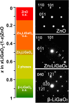
Phase variation in the (1 − x)ZnO–x(LiGaO2)1/2 pseudo-binary system together with the selected area electron diffraction (SAED) of ZnO, Zn2LiGaO4 and β-LiGaO2. The SAED patterns were recorded for the 〈formula image11〉 zone axis of the hexagonal wurtzite structure for ZnO and Zn2LiGaO4 and the 〈formula image01〉 zone axis of orthorhombic β-LiGaO2. The arrows in the SAED of Zn2LiGaO4 indicate superlattice diffractions.
Figure 3.
Figure 3.
Band gap variation as a function of x in the (1 − x)ZnO–x(LiGaO2)1/2 pseudo-binary system. The red dots and green dots indicate the band gaps determined for the ceramics and the films, respectively. The blue rectangle indicates a two phase region of Zn2LiGaO4 and β-LiGaO2 solid solutions. Although the boundary of the wurtzite-type phase and Zn2LiGaO4-type phase is between x = 0.1 and 0.2, all data are connected by one line, because both the phases are based on the wurtzite structure.
Figure 4.
Figure 4.
Variation of optical band gap of the (1 − x)ZnO–x(AgGaO2)1/2 alloys (red dots and line) as a function of the alloying level, x, together with that reported for the (1 − x)–xCdO alloys (green dots and line) for comparison.
Figure 5.
Figure 5.
Schematic illustration of the chemical bond between an oxide ion and a monovalent silver or copper ion in (a) β-AgGaO2 and (b) β-CuGaO2.
Figure 6.
Figure 6.
Optical absorption spectrum, F(Rd) of β-CuGaO2 obtained from the diffuse reflection, Rd, using the Kubelka–Munk function. Insets are a picture of powdered β-CuGaO2 and the theoretical conversion efficiency of a single-junction solar cell as a function of the band gap energy based on the Shockley–Queisser limit using the AM1.5G solar spectrum as the illumination source.
Figure 7.
Figure 7.
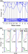
Electronic band structure of wurtzite-derived β-CuGaO2 calculated using the sX-LDA functional. (a) The band structure along the symmetry line and (b) the corresponding total and partial density of states.
Figure 8.
Figure 8.
Band gap versus pseudo-wurtzite lattice parameter, a0, for binary and ternary wurtzite-type oxide semiconductors.

References

    1. Ginley D S, Bright C. MRS Bull. 2000;8:15. doi: 10.1557/mrs2000.256. - DOI
    1. Ellmer K. Nat. Photon. 2012;6:809. doi: 10.1038/nphoton.2012.282. - DOI
    1. Minami T. Thin Solid Films. 2008;516:5822. doi: 10.1016/j.tsf.2007.10.063. - DOI - PubMed
    1. Fortunato E, Barquinha P, Martins R. Adv. Mater. 2012;24:2945. doi: 10.1002/adma.201103228. - DOI - PubMed
    1. Harrison W A. Electronic Structure and the Properties of Solids: The Physics of the Chemical Bond. New York: Dover; 1980.

LinkOut - more resources