Review
. 2008 Mar 13;9(1):014101.
doi: 10.1088/1468-6996/9/1/014101. eCollection 2008 Jan.

Highly spin-polarized materials and devices for spintronics

Affiliations
Review

Highly spin-polarized materials and devices for spintronics

Koichiro Inomata et al. Sci Technol Adv Mater. .

Abstract

The performance of spintronics depends on the spin polarization of the current. In this study half-metallic Co-based full-Heusler alloys and a spin filtering device (SFD) using a ferromagnetic barrier have been investigated as highly spin-polarized current sources. The multilayers were prepared by magnetron sputtering in an ultrahigh vacuum and microfabricated using photolithography and Ar ion etching. We investigated two systems of Co-based full-Heusler alloys, Co2Cr1 - x Fe x Al (CCFA(x)) and Co2FeSi1 - x Al x (CFSA(x)) and revealed the structure and magnetic and transport properties. We demonstrated giant tunnel magnetoresistance (TMR) of up to 220% at room temperature and 390% at 5 K for the magnetic tunnel junctions (MTJs) using Co2FeSi0.5Al0.5 (CFSA(0.5)) Heusler alloy electrodes. The 390% TMR corresponds to 0.81 spin polarization for CFSA(0.5) at 5 K. We also investigated the crystalline structure and local structure around Co atoms by x-ray diffraction (XRD) and nuclear magnetic resonance (NMR) analyses, respectively, for CFSA films sputtered on a Cr-buffered MgO (001) substrate followed by post-annealing at various temperatures in an ultrahigh vacuum. The disordered structures in CFSA films were clarified by NMR measurements and the relationship between TMR and the disordered structure was discussed. We clarified that the TMR of the MTJs with CFSA(0.5) electrodes depends on the structure, and is significantly higher for L21 than B2 in the crystalline structure. The second part of this paper is devoted to a SFD using a ferromagnetic barrier. The Co ferrite is investigated as a ferromagnetic barrier because of its high Curie temperature and high resistivity. We demonstrate the strong spin filtering effect through an ultrathin insulating ferrimagnetic Co-ferrite barrier at a low temperature. The barrier was prepared by the surface plasma oxidization of a CoFe2 film deposited on a MgO (001) single crystal substrate, wherein the spinel structure of CoFe2O4 (CFO) and an epitaxial relationship of MgO(001)[100]/CoFe2 (001)]110]/CFO(001)[100] were induced. A SFD consisting of CoFe2 /CFO/Ta on a MgO (001) substrate exhibits the inverse TMR of - 124% at 10 K when the configuration of the magnetizations of CFO and CoFe2 changes from parallel to antiparallel. The inverse TMR suggests the negative spin polarization of CFO, which is consistent with the band structure of CFO obtained by first principle calculation. The - 124% TMR corresponds to the spin filtering efficiency of 77% by the CFO barrier.

Keywords: Co-ferrites; Heusler alloys; magnetic tunnel junctions; nuclear magnetic resonance; spin filters; spin polarization.


Figures

Figure 1
Figure 1
Schematic representation of the DOS for a half metal.
Figure 2
Figure 2
L21 crystalline structure of full-Heusler alloys.
Figure 3
Figure 3
Spin-resolved DOS for Co2MnZ compound with Z = Al, Si, Ge and Sn [13].
Figure 4
Figure 4
Schematic illustration of origin of gap in minority bands in full-Heusler alloys. Here, d1, d2 and d3 denote the dxy, dyz and dzx orbitals, respectively, and d4 and d5 the d3z2-r2 and dx2-y2 orbitals, respectively [13].
Figure 5
Figure 5
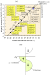
(a) Calculated total spin moments for full Heusler alloys. The dashed line represents the Slater–Pauling behavior. (b) Schematic band structure for explaining the Zt - 12 rule for total magnetization [13].
Figure 6
Figure 6
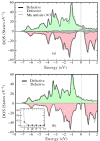
(a) Total DOS for defective (solid line) and ideal (dashed line) Co2MnSi with (a) Mn antisite and (b) Co antisite defects in Co2MnSi [14].
Figure 7
Figure 7
(a) XRD patterns obtained with Cu-Kα source for as-deposited Co2(Cr1 − xFex)Al films fabricated at RT on thermally oxidized Si substrates. The inset shows the (200) reflection intensity relative to that of the (220) peak. (b) Lattice constant as a function of x in Co2(Cr1 − xFex)Al films. The triangles represent the lattice constants for the bulk materials with x= 0 and 1 and the L21 structure.
Figure 8
Figure 8
X-ray reflectivity for 100 nm thick Co2 (Cr0.6Fe0.4) Al film deposited at RT and at elevated temperatures.
Figure 9
Figure 9
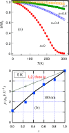
(a) Temperature dependence of magnetization for Co2Cr1 − xFexAl films with x= 1.0, 0.6, 0.4 and 0 from the top, and (b) Fe concentration dependence of the magnetic moment per formula unit estimated from the magnetization measurements at 5 K. The dotted line represents the theoretical values in the case of the L21 structure.
Figure 10
Figure 10
TMRs at RT and 5 K as a function of x for junctions with Co2Cr1 − xFexAl electrode.
Figure 11
Figure 11
TMR curves at RT and 5 K for junction with Co2 (Cr0.4 Fe0.6 )Al electrode.
Figure 12
Figure 12
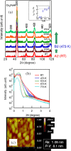
(a) XRD patterns and (b) x-ray reflectivity of Co2FeAl films deposited on SiO2 substrates at various temperatures. (c) AFM image of Co2FeAl deposited on SiO2 substrates at 773 K.
Figure 13
Figure 13
TMR and resistance-area (RA) product at RT as a function of substrate temperature for junctions with Co2FeAl electrode deposited on SiO2 substrates.
Figure 14
Figure 14
59Co NMR spectra for Co2FeAl films with A2 and B2 structures on SiO2 substrates.
Figure 15
Figure 15
(a) In-plane (upper) and out-of-plane (downward) XRDs for 20-nm-thick Co2FeAl films deposited on MgO substrates at various temperatures. (b) Intensity of (200) relative to that of (400). The broken line indicates the theoretical intensity.
Figure 16
Figure 16
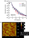
(a) X-ray reflectivity for Co2FeAl films deposited at various temperatures and (b) AFM image for the film deposited at 773 K on MgO (001) substrates.
Figure 17
Figure 17
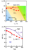
(a) TMR as a function of the substrate temperature for junctions deposited on SiO2 and MgO (001) substrates with a Co2FeAl electrode. (b) Temperature dependence of TMR for junctions deposited at RT on SiO2 and MgO (001) substrates with a Co2FeAl electrode.
Figure 18
Figure 18
In-plane (200) rocking curves for Co2FeSi and Co2FeAl thin films deposited on a MgO(100) substrate at 773 K.
Figure 19
Figure 19
TMR at RT as functions of the temperatures of substrate heating (Ts) and annealing (Ta) after deposition at RT for MgO(001)/Co2FeSi/AlOx /CoFe/IrMn/Ta junctions.
Figure 20
Figure 20
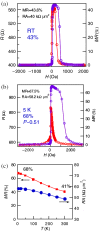
TMR curves at RT (a) and 5 K (b) for the MTJ with a Co2FeSi electrode. (c) Temperature dependence of TMR and RA.
Figure 21
Figure 21
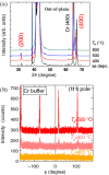
XRD patterns for (a) out-of-plane and (b) f scans for (111).
Figure 22
Figure 22
Surface roughness measured by AFM for CFSA films with various annealing temperatures.
Figure 23
Figure 23
TMR at RT as a function of post-annealing temperature for junctions with CFSA electrodes with different MgO layer thicknesses.
Figure 24
Figure 24
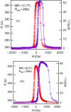
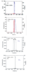
TMR curves at RT and 5 K for junctions with CFSA electrodes with post-annealing at (a) 430 °C and (b) 500 °C.
Figure 25
Figure 25
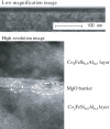
Cross-sectional TEM with low and high magnifications of the multilayer prepared under the same fabrication condition as the MTJ with 220% TMR.
Figure 26
Figure 26
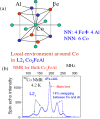
(a) Local structure around Co atom in L21-Co2FeAl. (b) 59Co NMR spectrum in bulk L21-Co2FeAl.
Figure 27
Figure 27
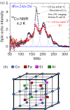
(a) NMR spectra for CFSA films on Cr-buffered MgO(001) for Ta = 400 ° C and 500 °C. (b) Ordered L21 structure of Co2FeSi0.5Al0.5.
Figure 28
Figure 28
Concept of spin-filtering device using an insulating ferromagnetic barrier.
Figure 29
Figure 29
Schematic of bias voltage dependence of TMR in a spin filter.
Figure 30
Figure 30
Calculated DOS for Co ferrite with inverse spinel structure.
Figure 31
Figure 31
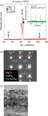
(a) In-plane XRD pattern for surface-oxidized CoFe2 films on MgO (001) single crystal substrates (oxidation time is 900 s). The inset shows φ scan on Co-ferrite 440 plane. (b) Electron diffraction pattern and (c) cross-sectional TEM image for MgO(001)/CoFe2 /Co-ferrite.
Figure 32
Figure 32
Hysteresis loops at RT for nonoxidized and oxidized CoFe2 thin films.
Figure 33
Figure 33
Tunneling magnetoresistance at (a) RT and (b) 5 K for spin filter consisting of CoFe2 /CoFe2-Ox.(600 s)/Ta (5 nm) on a MgO (001) single crystal substrate. The bias voltage is 5 mV.
Figure 34
Figure 34
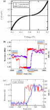
(a) Current density (J) – voltage (V) curve at 1 kOe (parallel state) at 10 K. The circles represent experimental data and solid line is curve fitted using Simmons equations. (b) Major R–H curve at 5 K and 5 mV and (c) minor R–H curve at 10 K and 1 mV for SFD consisting of CoFe2 (20 nm)-Ox. (900 s)/Ta (10 nm) on a MgO (001) single-crystal substrate.

References

    1. Butler W H, Zhang X-G, Schulthess T C. and MacLauren J M. Phys. Rev. 2001;63:054416.
    1. Mathon J. and Umersky A. Phys. Rev. 2001;63:220403R.
    1. Parkin S S, Kaiser C, Panchura A, Rice P M, Hughes B, Samant M. and Yang S H. Nat. Mater. 2004;3:862. doi: 10.1038/nmat1256. - DOI - PubMed
    1. Yuasa S, Fukushima A, Nagahama N, Ando K. and Suzuki Y. Nat. Mater. 2004;3:868. doi: 10.1038/nmat1257. - DOI - PubMed
    1. de Groot R A, Muller F M, van Engen P G. and Bushow K H J. Phys. Rev. Lett. 1983;50:2024. doi: 10.1103/PhysRevLett.50.2024. - DOI