Review
. 2008 May 15;8(5):3183-3204.
doi: 10.3390/s8053183.

Implantable Microimagers

Affiliations
Review

Implantable Microimagers

David C Ng et al. Sensors (Basel). .

Abstract

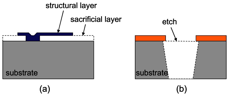
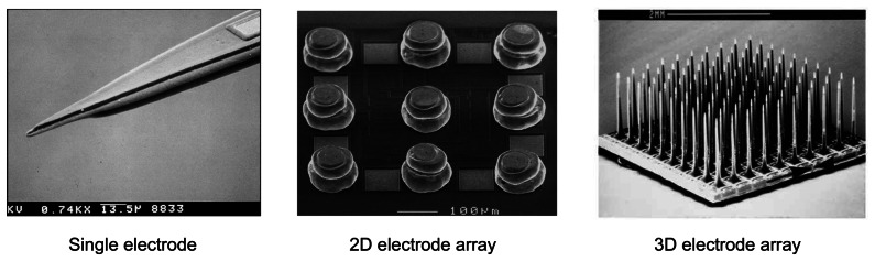
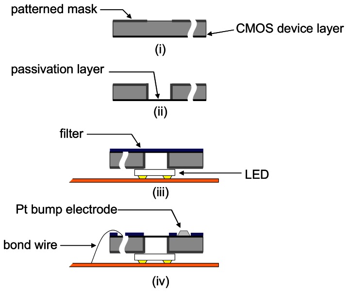
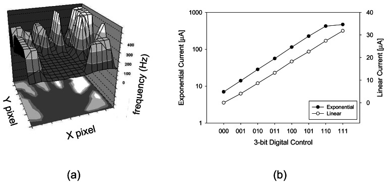
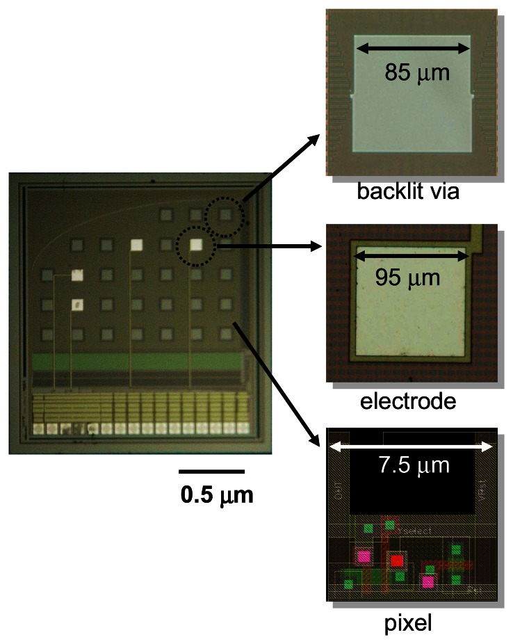
Implantable devices such as cardiac pacemakers, drug-delivery systems, and defibrillators have had a tremendous impact on the quality of live for many disabled people. To date, many devices have been developed for implantation into various parts of the human body. In this paper, we focus on devices implanted in the head. In particular, we describe the technologies necessary to create implantable microimagers. Design, fabrication, and implementation issues are discussed vis-à-vis two examples of implantable microimagers; the retinal prosthesis and in vivo neuro-microimager. Testing of these devices in animals verify the use of the microimagers in the implanted state. We believe that further advancement of these devices will lead to the development of a new method for medical and scientific applications.

Keywords: head; implant; in vivo.; microimager; retinal prosthesis.


Figures

Figure 1.
Figure 1.
Implantable microdevices in the head.
Figure 2.
Figure 2.
(a) Interconnection of photodiode and three transistor (M1, M2, M3) forming an active pixel sensor circuit. (b) Image sensor schematic based on three transistor APS circuit.
Figure 3.
Figure 3.
Typical microimager chip consisting of image sensor array, row and column scanners, and readout amplifiers (adapted from [40]).
Figure 4.
Figure 4.
Simplified cross-section schematic of typical CMOS technology (0.5 - 1 μm) with two-level metal interconnections.
Figure 5.
Figure 5.
Schematic cross-section of device undergone (a) surface, and (b) bulk micromachining.
Figure 6.
Figure 6.
Examples of single electrode [47] (© 2004 IEEE), 2D electrode array [38], and 3D electrode array [48] (© 1999 IEEE) fabricated using MEMS micromachining processes.
Figure 7.
Figure 7.
Post-processing of the sensor chip and packaging process flow of implantable device. (i) Pattern Al as mask for DRIE on backside of sensor chip, (ii) deep reactive ion etch backlit vias and sensor curved outline, (iii) attach sensor chip on top of flip-chip bonded LED, and spin coat optical filter, (vi) laser-assisted ablation of resist at bond sites followed by wire bonding of input output pads and forming Pt electrode onto Al electrodes. Finally device is sealed with transparent epoxy and precision laser cut out final shape (adapted from [11]).
Figure 8.
Figure 8.
Retinal prosthesis chip showing close-up of single pixel (adapted from [65]).
Figure 9.
Figure 9.
(a) Visualization of pulse output from 16×16 pixel array retinal prosthesis prototype chip based on pulse width modulation detection. (b) Stimulus current generated from a single electrode measured in saline (adapted from [65]).
Figure 10.
Figure 10.
Photographs of a fabricated microchip-based stimulator for retinal prosthesis. (a) close-up of the microchips, (b) bending of the stimulator, and (c) the stimulator with platinum wires covered with silicone tubing [64] (© 2006 IEEE).
Figure 11.
Figure 11.
In vivo microimager chip showing close-up of backlit via, electrode and pixel (adapted from [11]).
Figure 12.
Figure 12.
Microphotograph of fully packaged in vivo imager module. (a) close-up showing the image sensor and electrodes (inset), (b) LED illumination from integrated LED located under the sensor, and (c) full view of the device which is packaged onto a flexible polyimide substrate with printed interconnects (adapted from [11]).
Figure 13.
Figure 13.
(a) Fluorescence images captured after high frequency theta-burst stimulation in the hippocampus showing increase in protease activity. (b) Electric field potential recordings at various stimulation current strength by using the on-chip Pt electrodes.

References

    1. Greatbatch W., Holmes C.F. History of implantable devices. IEEE Eng. Med. Biol. 1991;10:38–41. 49. - PubMed
    1. Wilson B.S., Dorman M.F. Interfacing sensors with the nervous system: lessons from the development and success of the cochlear implant. IEEE Sensors J. 2008;1:131–147.
    1. Spelman F.A. Cochlear electrode arrays: past, present and future. Audiol. Neurotol. 2006;11:77–85. - PubMed
    1. Berger T.W., Baudry M., Brinton R.D., Liaw J.-S., Marmarelis V.Z., Yoondong Park A., Sheu B.J., Tanguay A.R., Jr. Brain-implantable biomimetic electronics as the next era in neuralprosthetics. P. IEEE. 2001;89:993–1012.
    1. Hochberg L.R., Serruya M.D., Friehs G.M., Mukand J.A., Saleh M., Caplan A.H., Branner A., Chen D., Penn R.D., Donoghue J.P. Neuronal ensemble control of prosthetic devices by a human with tetraplegia. Nature. 2006;442:164–171. - PubMed

LinkOut - more resources