

Fabrication and Characterization of Silicon Micro-Funnels and Tapered Micro-Channels for Stochastic Sensing Applications
- PMID: 27879912
- PMCID: PMC3924939
- DOI: 10.3390/s8063848
Fabrication and Characterization of Silicon Micro-Funnels and Tapered Micro-Channels for Stochastic Sensing Applications
Abstract
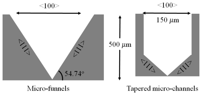
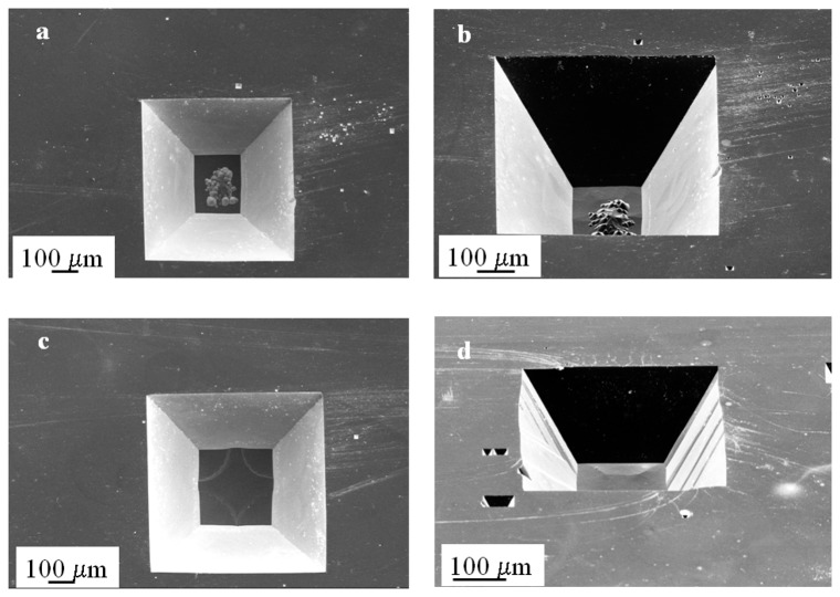
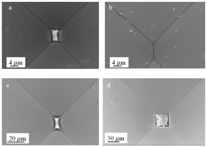
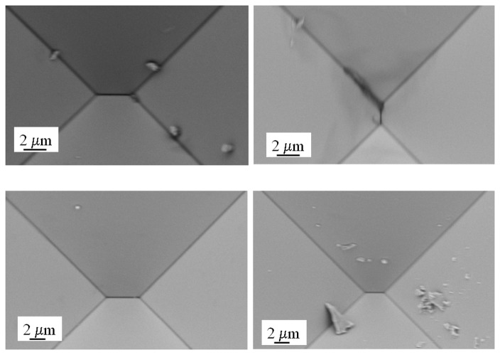
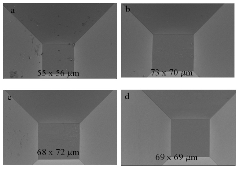
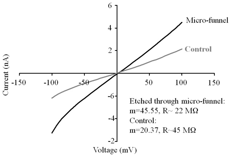
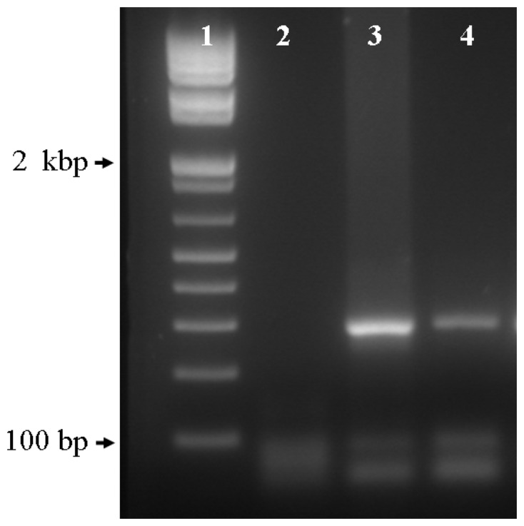
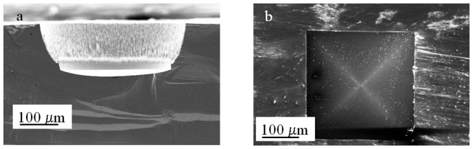
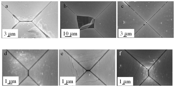
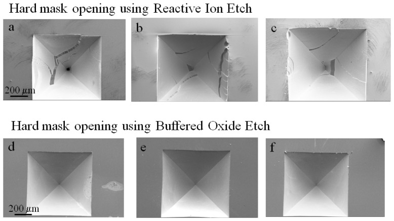
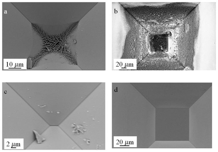
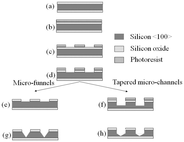
We present a simplified, highly reproducible process to fabricate arrays of tapered silicon micro-funnels and micro-channels using a single lithographic step with a silicon oxide (SiO2) hard mask on at a wafer scale. Two approaches were used for the fabrication. The first one involves a single wet anisotropic etch step in concentrated potassium hydroxide (KOH) and the second one is a combined approach comprising Deep Reactive Ion Etch (DRIE) followed by wet anisotropic etching. The etching is performed through a 500 mm thick silicon wafer, and the resulting structures are characterized by sharp tapered ends with a sub-micron cross-sectional area at the tip. We discuss the influence of various parameters involved in the fabrication such as the size and thickness variability of the substrate, dry and wet anisotropic etching conditions, the etchant composition, temperature, diffusion and micro-masking effects, the quality of the hard mask in the uniformity and reproducibility of the structures, and the importance of a complete removal of debris and precipitates. The presence of apertures at the tip of the structures is corroborated through current voltage measurements and by the translocation of DNA through the apertures. The relevance of the results obtained in this report is discussed in terms of the potential use of these structures for stochastic sensing.
Keywords: anisotropic etching.; silicon; stochastic sensing.
Figures
Similar articles
-
Aluminum oxide mask fabrication by focused ion beam implantation combined with wet etching.Nanotechnology. 2013 May 3;24(17):175304. doi: 10.1088/0957-4484/24/17/175304. Epub 2013 Apr 9. Nanotechnology. 2013. PMID: 23571491
-
Two-Layer Microstructures Fabricated by One-Step Anisotropic Wet Etching of Si in KOH Solution.Micromachines (Basel). 2016 Jan 25;7(2):19. doi: 10.3390/mi7020019. Micromachines (Basel). 2016. PMID: 30407392 Free PMC article.
-
Fabrication of arrays of tapered silicon micro-/nano-pillars by metal-assisted chemical etching and anisotropic wet etching.Nanotechnology. 2018 Jul 13;29(28):28LT01. doi: 10.1088/1361-6528/aac04b. Epub 2018 Apr 26. Nanotechnology. 2018. PMID: 29697051
-
Voltage- and Metal-assisted Chemical Etching of Micro and Nano Structures in Silicon: A Comprehensive Review.Small. 2024 Aug;20(35):e2400499. doi: 10.1002/smll.202400499. Epub 2024 Apr 21. Small. 2024. PMID: 38644330 Review.
-
A Thorough Review of Emerging Technologies in Micro- and Nanochannel Fabrication: Limitations, Applications, and Comparison.Micromachines (Basel). 2024 Oct 21;15(10):1274. doi: 10.3390/mi15101274. Micromachines (Basel). 2024. PMID: 39459148 Free PMC article. Review.
Cited by
-
A Fluidic Interface with High Flow Uniformity for Reusable Large Area Resonant Biosensors.Micromachines (Basel). 2017 Oct 14;8(10):308. doi: 10.3390/mi8100308. Micromachines (Basel). 2017. PMID: 30400497 Free PMC article.
-
Anisotropic diamond etching through thermochemical reaction between Ni and diamond in high-temperature water vapour.Sci Rep. 2018 Apr 27;8(1):6687. doi: 10.1038/s41598-018-25193-2. Sci Rep. 2018. PMID: 29703922 Free PMC article.
References
-
- Madou M. Fundamentals of Microfabrication. R. Powers; New York: 1997. p. 145.
-
- Kovacs G.T.A. Micromachined Transducers Sourcebook. T. Casso; U.S.A: 1998. p. 29.
-
- Ziaie B., Baldi A., Lei M., Gu Y., Siegel R.A. Hard and soft micromachining for BioMEMS: review of techniques and examples of applications in microfluidics and drug delivery. Adv. Drug Deliver Rev. 2004;56:145–172. - PubMed
-
- Bean K.E. Anisotropic Etching of Silicon. IEEE T. Electron Dev. 1978;ED-25:1185–1193.
-
- Vaganov V. Method for fabrication microstructures with deep anisotropic etching of thick silicon wafers. United States Patent No. 6,787,052 2004
LinkOut - more resources
Full Text Sources
Other Literature Sources
