. 2016 Dec;11(1):525.
doi: 10.1186/s11671-016-1731-z. Epub 2016 Nov 25.

Structural and electronic properties of two-dimensional stanene and graphene heterostructure

Affiliations

Structural and electronic properties of two-dimensional stanene and graphene heterostructure

Liyuan Wu et al. Nanoscale Res Lett. 2016 Dec.

Abstract

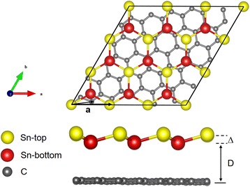
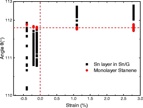
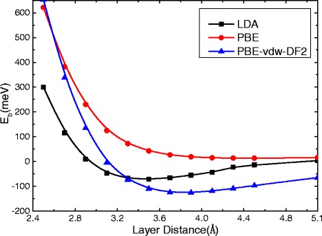
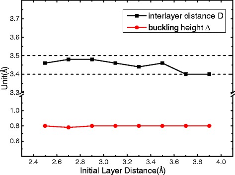
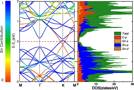
Structural and electronic properties of two-dimensional stanene and graphene heterostructure (Sn/G) are studied by using first-principles calculations. Various supercell models are constructed in order to reduce the strain induced by the lattice mismatch. The results show that stanene interacts overall weakly with graphene via van der Waals (vdW) interactions. Multiple phases of different crystalline orientation of stanene and graphene could coexist at room temperature. Moreover, interlayer interactions in stanene and graphene heterostructure can induce tunable band gaps at stanene's Dirac point, and weak p-type and n-type doping of stanene and graphene, respectively, generating a small amount of electron transfer from stanene to graphene. Interestingly, for model [Formula: see text] , there emerges a band gap about 34 meV overall the band structure, indicating it shows semiconductor feature.

Keywords: First-principles; Graphene; Heterostructure; Stanene; Structural properties.


Figures

Fig. 1
Fig. 1
Top and side views of the heterostructure of Sn3/G31 (a heterostructure consisting of 3 × 3 stanene unit cell and 31×31 graphene unit cell). Yellow, red, and gray spheres represent Sn-top, Sn-bottom, and C atoms, respectively. Δ and D represent the buckling height of stanene and interlayer distance between the substrate graphene and bottom Sn layer, respectively. The black arrows represent the lattice vector aSnandaG and of the unit cell of stanene and graphene
Fig. 2
Fig. 2
Distribution of the bond angles in Sn layer of different heterostructure models in Table 1 and corresponding monolayer stanene
Fig. 3
Fig. 3
Interlayer binding energy per Sn atom of the bilayer Sn7/G5 as a function of interlayer spacing. Results using different exchange-correlation functionals are shown. See text for the geometry and the binding energy definition
Fig. 4
Fig. 4
Equilibrium interlayer distance D of the bilayer Sn(7)/G(5) and buckling height Δ of Sn layer obtained from optimized structure of different initial interlayer distance
Fig. 5
Fig. 5
Binding energy (per Sn atom) E b and energy per Sn in comparison with the bulk value E c for stanene on graphene obtained using various supercell models in Table 1. The results (a E c and b E b) are plotted as a function of strain in the layer
Fig. 6
Fig. 6
Electronic structures of the a monolayer graphene, b monolayer stanene, and c bilayer Sn3/G31. The red line represents the Fermi level, which set to be zero. The relative contribution of stanene is coded by color: blue (red) corresponds to the state originating only from stanene (graphene). The substrate-induced gap is 67 meV for Sn (Γ) and 3 meV for graphene (K)
Fig. 7
Fig. 7
Band structure of a Sn7/G5, the Dirac point of them both located at K, b Sn13/G43, the Dirac point of stanene (graphene) is located at K (Γ), c Sn21/G73, the Dirac point of stanene (graphene) is located at Γ (K), and d Sn27/G97, the Dirac points of stanene and graphene are both located at K
Fig. 8
Fig. 8
Electronic band structure and DOS of Sn7/G5. The relative contribution of stanene is coded by color: blue (red) corresponds to the state originating only from stanene (graphene)

References

    1. Novoselov KS, Geim AK, Morozov SV, Jiang D, Zhang Y, Dubonos SV, Firsov AA, et al. Electric field effect in atomically thin carbon films. Science. 2004;306:666–669. doi: 10.1126/science.1102896. - DOI - PubMed
    1. Geim AK, Novoselov KS. The rise of graphene. Nat Mater. 2007;6:183–191. doi: 10.1038/nmat1849. - DOI - PubMed
    1. Zhang S, Zhou J, Wang Q, Chen X, Kawazoe Y, Jena P. Penta-graphene: a new carbon allotrope. Proc Natl Acad Sci. 2015;112(8):2372–2377. doi: 10.1073/pnas.1416591112. - DOI - PMC - PubMed
    1. Wang FQ, Yu J, Wang Q, Kawazoe Y, Jena P. Lattice thermal conductivity of penta-graphene. Carbon. 2016;105:424–429. doi: 10.1016/j.carbon.2016.04.054. - DOI
    1. Li X, Zhang S, Wang FQ, Guo Y, Liu J, Wang Q. Tuning the electronic and mechanical properties of penta-graphene via hydrogenation and fluorination. Phys Chem Chem Phys. 2016;18(21):14191–14197. doi: 10.1039/C6CP01092J. - DOI - PubMed

LinkOut - more resources