. 2016 Nov 28:6:37296.
doi: 10.1038/srep37296.

Current induced polycrystalline-to-crystalline transformation in vanadium dioxide nanowires

Affiliations

Current induced polycrystalline-to-crystalline transformation in vanadium dioxide nanowires

Junho Jeong et al. Sci Rep. .

Abstract

Vanadium dioxide (VO2) exhibits a reversible insulator-metal phase transition that is of significant interest in energy-efficient nanoelectronic and nanophotonic devices. In these applications, crystalline materials are usually preferred for their superior electrical transport characteristics as well as spatial homogeneity and low surface roughness over the device area for reduced scattering. Here, we show applied electrical currents can induce a permanent reconfiguration of polycrystalline VO2 nanowires into crystalline nanowires, resulting in a dramatically reduced hysteresis across the phase transition and reduced resistivity. Low currents below 3 mA were sufficient to cause the local temperature in the VO2 to reach about 1780 K to activate the irreversible polycrystalline-to-crystalline transformation. The crystallinity was confirmed by electron microscopy and diffraction analyses. This simple yet localized post-processing of insulator-metal phase transition materials may enable new methods of studying and fabricating nanoscale structures and devices formed from these materials.


Figures

Figure 1
Figure 1. The fabricated device and the as-sputtered VO2 film.
The (a) top and (b) cross-section view schematics of a VO2 device with Pd contacts. (c) SEM images of a device at two magnifications. (d) X-ray diffraction pattern of the starting VO2 film before crystallization.
Figure 2
Figure 2. VI and resistivity measurements before and after crystallization.
VI measurements for (a) L = 0.77 μm and W = 2.4 μm and (b) L = 0.99 μm and W = 0.93 μm. (c) The resistivity vs. current corresponding to (a) and the inset is the magnified region in dashed lines. (d) The resistivity vs. temperature for the “before” and “after” states showing the reduced hysteresis and resistivity in the “after” state.
Figure 3
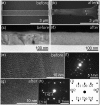
Figure 3. Electron microscopy images and diffraction patterns before and after the crystallization.
Top view SEM images of the VO2 nanowire device with L = 7.5 μm and W = 0.91 μm (a) before and (b) after the crystallization. XTEM images of a VO2 nanowire (c) before and (d) after crystallization showing the absence of grains in the “after” state. (e) is the high-resolution TEM and (f) the SAED pattern corresponding to the “before” state in (c). The polycrystallinity is evident in the non-uniform plane orientations in (e) and randomness of the diffraction pattern in (f). (g) is the high-resolution TEM and (h) the SAED pattern corresponding to the “after” state in (d) taken in the VO2 metallic (rutile) phase. The atomic arrangement is more periodic and the diffraction pattern exhibits clear symmetries that can be matched to the (i) computed diffraction pattern of VO2 with a rutile crystal structure at view direction [210] using the lattice parameters from ref. .
Figure 4
Figure 4. Thermal modeling of the crystallization.
(a) The measured dissipated power at the critical current compared to the power required to heat the VO2 nanowires by ΔT = 1470 K calculated using (a) 1D Fourier model for devices with varying W/L. The result of a thermal transport simulation (COMSOL Multiphysics) showing (b) the current density and (c) temperature distribution for VO2 wire of dimensions L = 0.78 μm and W = 0.41 μm at the critical current, IC.

References

    1. Shibuya K., Ohnishi T., Lippmaa M., Kawasaki M. & Koinuma H. Single crystal SrTiO3 field-effect transistor with an atomically flat amorphous CaHfO3 gate insulator. Applied Physics Letters 85, 425–427 (2004).
    1. Zhou Y. & Ramanathan S. Correlated Electron Materials and Field Effect Transistors for Logic: A Review. Critical Reviews in Solid State and Materials Sciences 38, 286–317 (2013).
    1. Shukla N. et al.. A steep-slope transistor based on abrupt electronic phase transition. Nature communications 6, 7812 (2015). - PMC - PubMed
    1. Driscoll T., Kim H. T., Chae B. G., Di Ventra M. & Basov D. N. Phase-transition driven memristive system. Applied Physics Letters 95, 2–4 (2009).
    1. Ha S. D., Aydogdu G. H. & Ramanathan S. Metal-insulator transition and electrically driven memristive characteristics of SmNiO3 thin films. Applied Physics Letters 98, 98–101 (2011).

Publication types