Fluorinated benzalkylsilane molecular rectifiers
- PMID: 27897250
- PMCID: PMC5126687
- DOI: 10.1038/srep38092
Fluorinated benzalkylsilane molecular rectifiers
Abstract
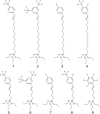
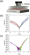
We report on the synthesis and electrical properties of nine new alkylated silane self-assembled monolayers (SAMs) - (EtO)3Si(CH2)nN = CHPhX where n = 3 or 11 and X = 4-CF3, 3,5-CF3, 3-F-4-CF3, 4-F, or 2,3,4,5,6-F, and explore their rectification behavior in relation to their molecular structure. The electrical properties of the films were examined in a metal/insulator/metal configuration, with a highly-doped silicon bottom contact and a eutectic gallium-indium liquid metal (EGaIn) top contact. The junctions exhibit high yields (>90%), a remarkable resistance to bias stress, and current rectification ratios (R) between 20 and 200 depending on the structure, degree of order, and internal dipole of each molecule. We found that the rectification ratio correlates positively with the strength of the molecular dipole moment and it is reduced with increasing molecular length.
Figures


References
-
- Collier C. P. Electronically Configurable Molecular-Based Logic Gates. Science 285, 391–394 (1999). - PubMed
-
- Reed M. A., Chen J., Rawlett A. M., Price D. W. & Tour J. M. Molecular random access memory cell. Appl. Phys. Lett. 78, 3735 (2001).
-
- Green J. E. et al.. A 160-kilobit molecular electronic memory patterned at 10(11) bits per square centimetre. Nature 445, 414–417 (2007). - PubMed
-
- Rascón-Ramos H., Artés J. M., Li Y. & Hihath J. Binding configurations and intramolecular strain in single-molecule devices. Nat. Mater. 14, 1–6 (2015). - PubMed
-
- Haedler A. T. et al.. Long-range energy transport in single supramolecular nanofibres at room temperature. Nature 523, 196–199 (2015). - PubMed
Publication types
LinkOut - more resources
Full Text Sources
Other Literature Sources

