

Electrical Properties of Ultrathin Hf-Ti-O Higher k Gate Dielectric Films and Their Application in ETSOI MOSFET
- PMID: 27905095
- PMCID: PMC5130927
- DOI: 10.1186/s11671-016-1754-5
Electrical Properties of Ultrathin Hf-Ti-O Higher k Gate Dielectric Films and Their Application in ETSOI MOSFET
Abstract
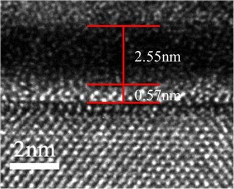
Ultrathin Hf-Ti-O higher k gate dielectric films (~2.55 nm) have been prepared by atomic layer deposition. Their electrical properties and application in ETSOI (fully depleted extremely thin SOI) PMOSFETs were studied. It is found that at the Ti concentration of Ti/(Ti + Hf) ~9.4%, low equivalent gate oxide thickness (EOT) of ~0.69 nm and acceptable gate leakage current density of 0.61 A/cm2 @ (V fb - 1)V could be obtained. The conduction mechanism through the gate dielectric is dominated by the F-N tunneling in the gate voltage range of -0.5 to -2 V. Under the same physical thickness and process flow, lower EOT and higher I on/I off ratio could be obtained while using Hf-Ti-O as gate dielectric compared with HfO2. With Hf-Ti-O as gate dielectric, two ETSOI PMOSFETs with gate width/gate length (W/L) of 0.5 μm/25 nm and 3 μm/40 nm show good performances such as high I on, I on/I off ratio in the magnitude of 105, and peak transconductance, as well as suitable threshold voltage (-0.3~-0.2 V). Particularly, ETSOI PMOSFETs show superior short-channel control capacity with DIBL <82 mV/V and subthreshold swing <70 mV/decade.
Keywords: Atomic layer deposition; ETSOI MOSFET; Electrical properties; Higher k; Ultrathin Hf-Ti-O gate dielectric films.
Figures
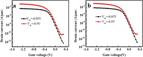
 V
ds = −0.9 V). a With HfO2 as gate dielectric. b With Hf-Ti-O as gate dielectric
V
ds = −0.9 V). a With HfO2 as gate dielectric. b With Hf-Ti-O as gate dielectric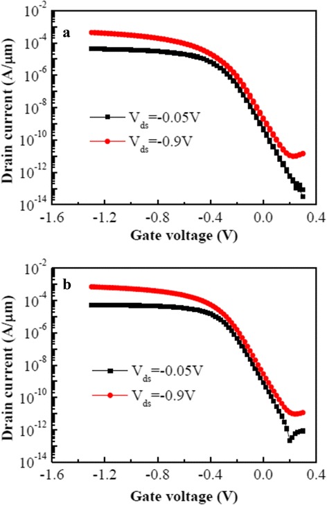
 V
ds = −0.9 V). a
W/L = 0.5 μm/25 nm. b
W/L = 3 μm/40 nm
V
ds = −0.9 V). a
W/L = 0.5 μm/25 nm. b
W/L = 3 μm/40 nm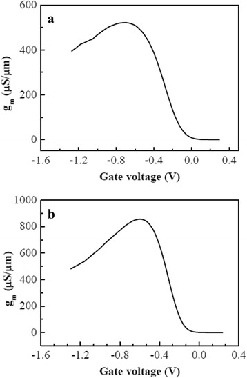
Similar articles
-
Near-ideal subthreshold swing MoS2 back-gate transistors with an optimized ultrathin HfO2 dielectric layer.Nanotechnology. 2019 Mar 1;30(9):095202. doi: 10.1088/1361-6528/aaf956. Epub 2018 Dec 18. Nanotechnology. 2019. PMID: 30561381
-
Parametric Analysis of Indium Gallium Arsenide Wafer-based Thin Body (5 nm) Double-gate MOSFETs for Hybrid RF Applications.Recent Pat Nanotechnol. 2024;18(3):335-349. doi: 10.2174/1872210517666230602095347. Recent Pat Nanotechnol. 2024. PMID: 37723950
-
Effects of HfO2 encapsulation on electrical performances of few-layered MoS2 transistor with ALD HfO2 as back-gate dielectric.Nanotechnology. 2018 Aug 24;29(34):345201. doi: 10.1088/1361-6528/aac853. Epub 2018 May 29. Nanotechnology. 2018. PMID: 29808825
-
Comprehensive Study of Lanthanum Aluminate High-Dielectric-Constant Gate Oxides for Advanced CMOS Devices.Materials (Basel). 2012 Mar 14;5(3):443-477. doi: 10.3390/ma5030443. Materials (Basel). 2012. PMID: 28817057 Free PMC article. Review.
-
Ultimate Scaling of High-κ Gate Dielectrics: Higher-κ or Interfacial Layer Scavenging?Materials (Basel). 2012 Mar 14;5(3):478-500. doi: 10.3390/ma5030478. Materials (Basel). 2012. PMID: 28817058 Free PMC article. Review.
Cited by
-
Integration of Highly Strained SiGe in Source and Drain with HK and MG for 22 nm Bulk PMOS Transistors.Nanoscale Res Lett. 2017 Dec;12(1):123. doi: 10.1186/s11671-017-1908-0. Epub 2017 Feb 16. Nanoscale Res Lett. 2017. PMID: 28228008 Free PMC article.
References
-
- Semiconductor Industry Association. National technology roadmap for semiconductors. ITRS 2013, ITRS 2009, http://www.itrs2.net/
-
- Mistry K, Allen C, Auth C, Beattie B, et al. A 45nm logic technology with high-k + metal gate transistors, strained silicon, 9 Cu interconnect layers, 193 nm dry patterning, and 100% Pb-free packaging. Washington: IEEE, 2007; 2007. pp. 247–250.
-
- Frank MM. Proceedings of the European solid-state circuits conference. Helsinki: IEEE, 2011; 2011. pp. 25–33.
-
- Li M, Zhang Z, Campbell SA, Gladfelter WL, et al. Electrical and material characterizations of high-permittivity HfxTi1-xO2 gate insulators. J Appl Phys. 2005;98(5):054506. doi: 10.1063/1.2039268. - DOI
LinkOut - more resources
Full Text Sources
Other Literature Sources
Research Materials
Miscellaneous
