

Epitaxy of highly ordered organic semiconductor crystallite networks supported by hexagonal boron nitride
- PMID: 27929042
- PMCID: PMC5143978
- DOI: 10.1038/srep38519
Epitaxy of highly ordered organic semiconductor crystallite networks supported by hexagonal boron nitride
Erratum in
-
Corrigendum: Epitaxy of highly ordered organic semiconductor crystallite networks supported by hexagonal boron nitride.Sci Rep. 2017 May 3;7:46794. doi: 10.1038/srep46794. Sci Rep. 2017. PMID: 28467394 Free PMC article. No abstract available.
Abstract
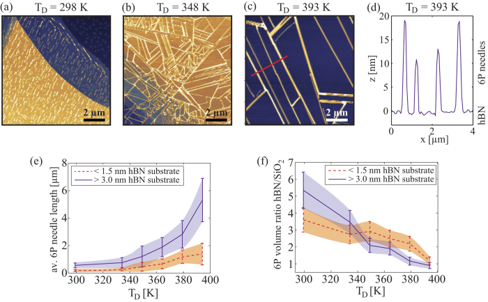
This study focuses on hexagonal boron nitride as an ultra-thin van der Waals dielectric substrate for the epitaxial growth of highly ordered crystalline networks of the organic semiconductor parahexaphenyl. Atomic force microscopy based morphology analysis combined with density functional theory simulations reveal their epitaxial relation. As a consequence, needle-like crystallites of parahexaphenyl grow with their long axes oriented five degrees off the hexagonal boron nitride zigzag directions. In addition, by tuning the deposition temperature and the thickness of hexagonal boron nitride, ordered networks of needle-like crystallites as long as several tens of micrometers can be obtained. A deeper understanding of the organic crystallites growth and ordering at ultra-thin van der Waals dielectric substrates will lead to grain boundary-free organic field effect devices, limited only by the intrinsic properties of the organic semiconductors.
Figures
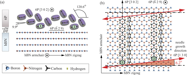
 6P contact plane with hBN basal plane, (a) side view of the interface, and (b) top view. Molecules closest to the hBN surface are labeled with the numbers 1 and 2. Red arrows in (b) represent the 6P [130] direction that corresponds to the long axis of the resulting 6P needles.
Similar articles
-
Highly Ordered Boron Nitride/Epigraphene Epitaxial Films on Silicon Carbide by Lateral Epitaxial Deposition.ACS Nano. 2020 Oct 27;14(10):12962-12971. doi: 10.1021/acsnano.0c04164. Epub 2020 Oct 1. ACS Nano. 2020. PMID: 32966058
-
Epitaxial growth of molecular crystals on van der waals substrates for high-performance organic electronics.Adv Mater. 2014 May;26(18):2812-7. doi: 10.1002/adma.201304973. Epub 2014 Jan 23. Adv Mater. 2014. PMID: 24458727
-
Van der Waals epitaxy and characterization of hexagonal boron nitride nanosheets on graphene.Nanoscale Res Lett. 2014 Jul 28;9(1):367. doi: 10.1186/1556-276X-9-367. eCollection 2014. Nanoscale Res Lett. 2014. PMID: 25114656 Free PMC article.
-
Hexagonal Boron Nitride Based Photonic Quantum Technologies.Materials (Basel). 2024 Aug 20;17(16):4122. doi: 10.3390/ma17164122. Materials (Basel). 2024. PMID: 39203299 Free PMC article. Review.
-
Van der Waals Epitaxy of III-Nitride Semiconductors Based on 2D Materials for Flexible Applications.Adv Mater. 2020 Apr;32(15):e1903407. doi: 10.1002/adma.201903407. Epub 2019 Sep 5. Adv Mater. 2020. PMID: 31486182 Review.
Cited by
-
Quantitative determination of a model organic/insulator/metal interface structure.Nanoscale. 2018 Nov 29;10(46):21971-21977. doi: 10.1039/c8nr06387g. Nanoscale. 2018. PMID: 30444513 Free PMC article.
-
Photoinduced edge-specific nanoparticle decoration of two-dimensional tungsten diselenide nanoribbons.Commun Chem. 2023 Aug 14;6(1):166. doi: 10.1038/s42004-023-00975-6. Commun Chem. 2023. PMID: 37580376 Free PMC article.
-
Probing charge transfer between molecular semiconductors and graphene.Sci Rep. 2017 Aug 25;7(1):9544. doi: 10.1038/s41598-017-09419-3. Sci Rep. 2017. PMID: 28842584 Free PMC article.
-
Highly distinguishable isomeric states of a tripodal arylazopyrazole derivative on graphite through electron/hole-induced switching at ambient conditions.Beilstein J Org Chem. 2025 Jul 22;21:1496-1507. doi: 10.3762/bjoc.21.112. eCollection 2025. Beilstein J Org Chem. 2025. PMID: 40726596 Free PMC article.
References
-
- Shirakawa H., Louis E. J., MacDiarmid A. G., Chiang C. K. & Heeger A. J. Synthesis of electrically conducting organic polymers: halogen derivatives of polyacetylene, (CH)x. J. Chem. Soc., Chem. Commun. 16, 578–580 (1977).
-
- Park Y. D., Lim J. A., Lee H. S. & Cho K. Interface engineering in organic transistors. Mater. Today 10, 46–54 (2007).
-
- Di C.-a., Liu Y., Yu G. & Zhu D. Interface engineering: an effective approach toward high-performance organic field-effect transistors. Accounts Chem. Res. 42, 1573–1583 (2009). - PubMed
-
- Jurchescu O. D., Popinciuc M., van Wees B. J. & Palstra T. T. Interface-controlled, high-mobility organic transistors. Adv. Mater. 19, 688–692 (2007).
-
- Zhang Y. et al.. Probing carrier transport and structure-property relationship of highly ordered organic semiconductors at the two-dimensional limit. Phys. Rev. Lett. 116, 016602 (2016). - PubMed
Publication types
Grants and funding
LinkOut - more resources
Full Text Sources
Other Literature Sources
Research Materials
