Review
. 2017 Jan 25;117(2):796-837.
doi: 10.1021/acs.chemrev.6b00215. Epub 2016 Dec 7.

Light Harvesting for Organic Photovoltaics

Affiliations
Review

Light Harvesting for Organic Photovoltaics

Gordon J Hedley et al. Chem Rev. .

Abstract

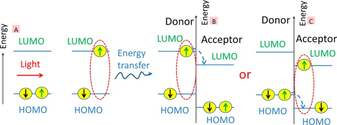
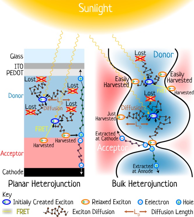
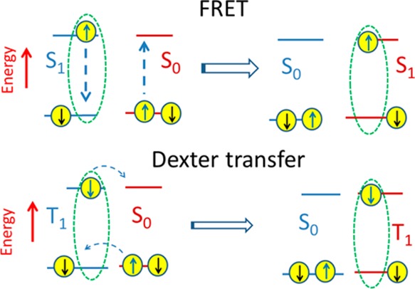
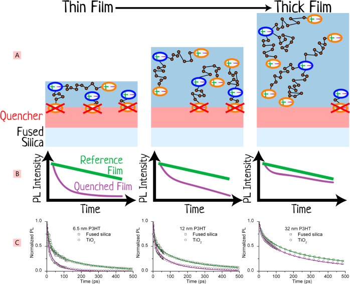
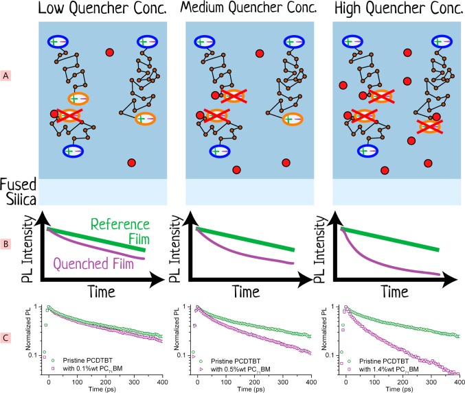
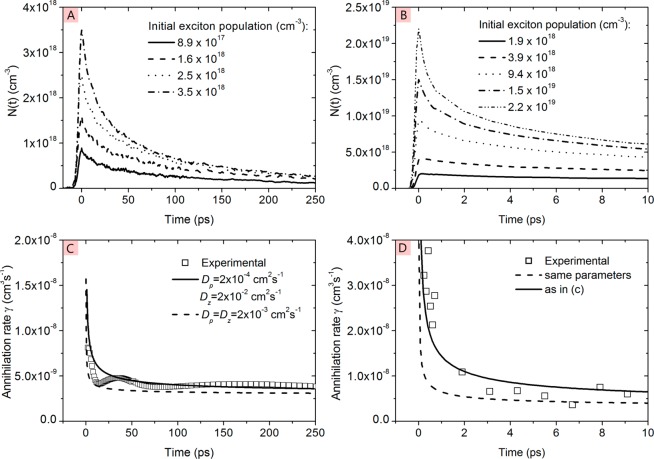
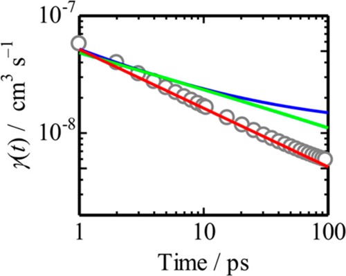
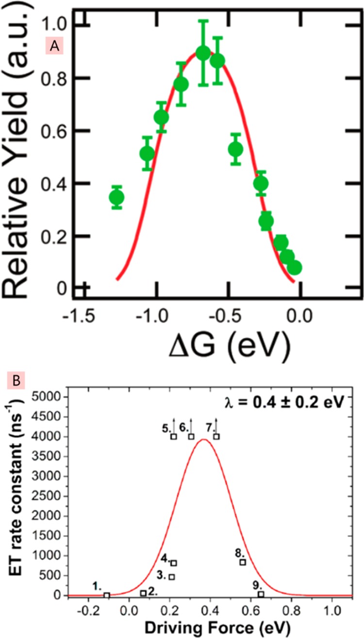
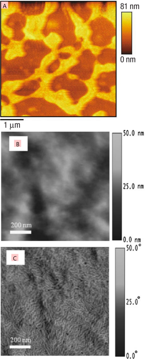
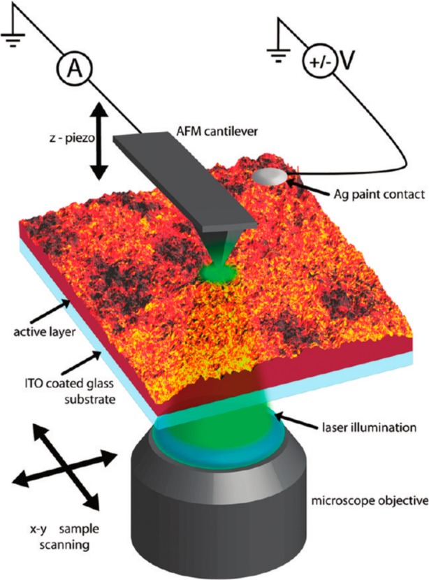
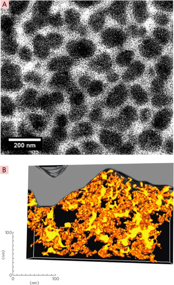
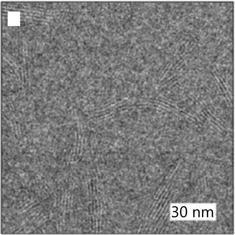
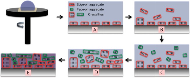
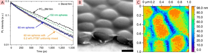
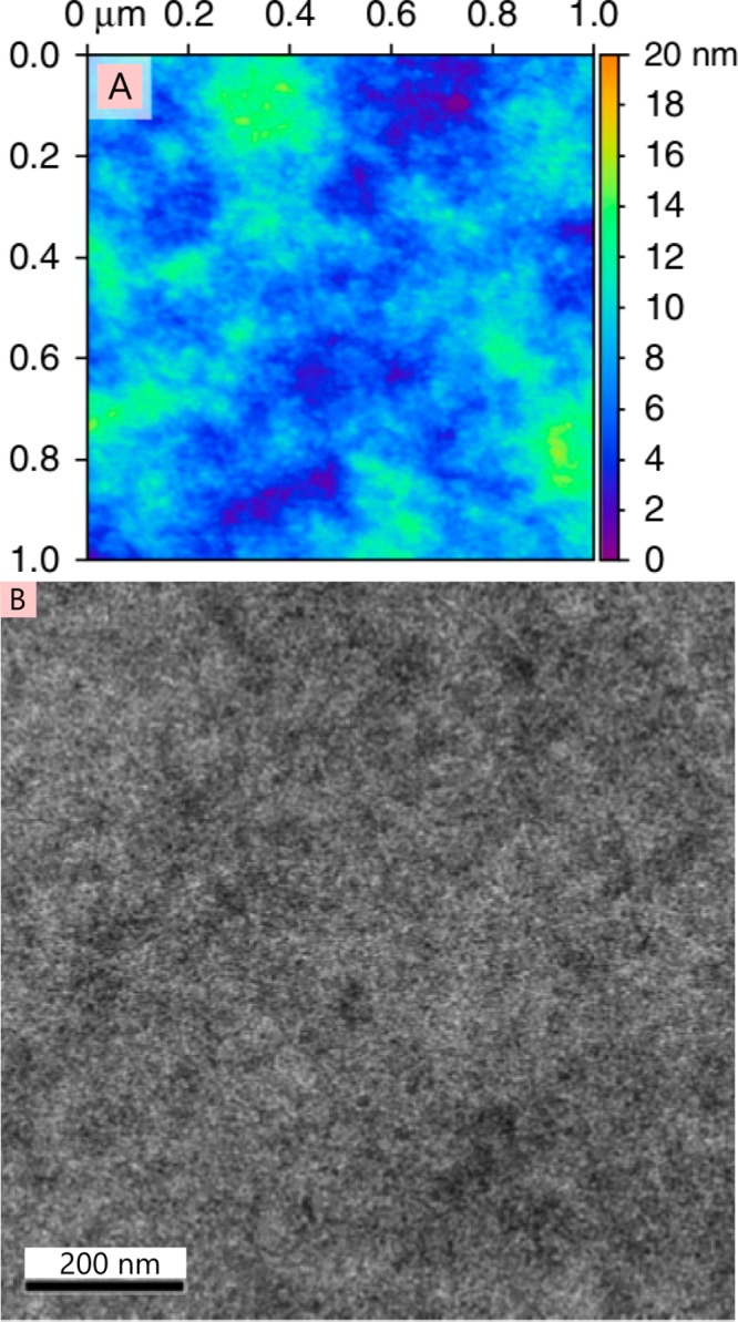
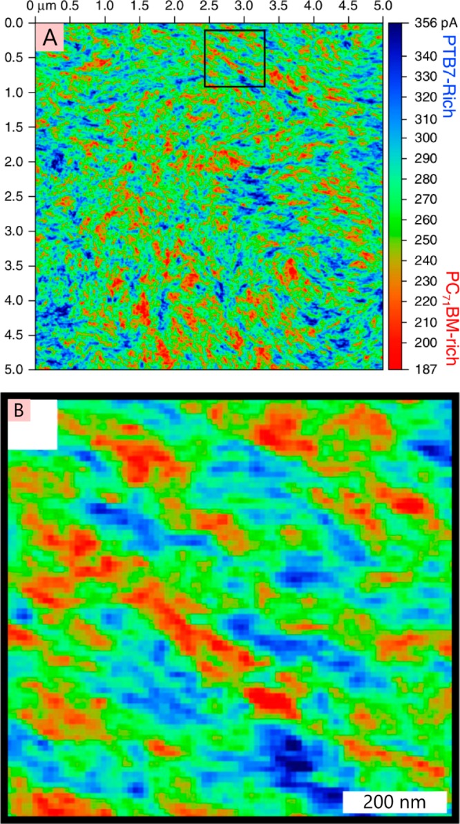
The field of organic photovoltaics has developed rapidly over the last 2 decades, and small solar cells with power conversion efficiencies of 13% have been demonstrated. Light absorbed in the organic layers forms tightly bound excitons that are split into free electrons and holes using heterojunctions of electron donor and acceptor materials, which are then extracted at electrodes to give useful electrical power. This review gives a concise description of the fundamental processes in photovoltaic devices, with the main emphasis on the characterization of energy transfer and its role in dictating device architecture, including multilayer planar heterojunctions, and on the factors that impact free carrier generation from dissociated excitons. We briefly discuss harvesting of triplet excitons, which now attracts substantial interest when used in conjunction with singlet fission. Finally, we introduce the techniques used by researchers for characterization and engineering of bulk heterojunctions to realize large photocurrents, and examine the formed morphology in three prototypical blends.


Conflict of interest statement

The authors declare no competing financial interest.

Figures

Figure 1
Figure 1
Schematic illustration of charge generation in organic photovoltaic materials which involves (A) light absorption and the generation of a singlet exciton with opposite “up” and “down” spins, followed by energy transfer to a type II heterojunction of an electron donor and acceptor and then (B) electron or (C) hole transfer at the heterojunction. Charge transfer can also occur from triplet excitons if the energy level offset is sufficient.
Figure 2
Figure 2
The two main architectures of organic photovoltaic devices and the processes occurring in them (not to scale). On the left is a cross section of a planar heterojunction; on the right is a magnified region of a bulk heterojunction. In both diagrams, the donor region is light blue and the acceptor region is red, and the key defines the other elements. Sunlight incident on the devices leads to the formation of excitons that then diffuse (and/or transfer energy by FRET) to the heterojunction where charge separation occurs. Some excitons do not reach the heterojunction and are lost. These processes are discussed in more detail throughout the review.
Figure 3
Figure 3
Schematic illustration of nonradiative Förster resonance energy transfer of singlet exciton S1 and Dexter transfer of triplet exciton T1. The “up” and “down” arrows illustrate electron spins, and S0 denotes a chromophore in the ground state.
Figure 4
Figure 4
Schematic of the surface quenching technique. (A) Varying thicknesses of the material of interest (blue block in the stack) are deposited on top of a quencher material (red block), and the time-resolved PL decays are measured (schematically shown in panel B) and compared against a reference film of the material prepared without the quencher layer. The thickness dependence of the time-resolved quenching can be used to determine the exciton diffusion coefficient. Shown in panel C are experimental data of surface quenching in 6.5, 12, and 32 nm thick films of the polymer P3HT deposited on titania (the quencher). Panel C is modified and reprinted with permission from ref (65). Copyright 2008 John Wiley and Sons.
Figure 5
Figure 5
Fluorescence quenching efficiency in the 26 nm polymer film as a function of time after evaporation of C60 on top. The C60 evaporation starts at t = 0. The inset shows the increase of the apparent exciton diffusion distance with time, which indicates intermixing of the evaporated C60 molecules with the soft polymer layer. This leads to an overestimate of the intrinsic exciton diffusion length. Reprinted with permission from ref (67). Copyright 2005 American Chemical Society.
Figure 6
Figure 6
Schematic illustration of the volume-quenching technique in which quenchers are dispersed throughout the layer of the material to be studied. Shown in panel A from left to right are three films of the material under investigation (blue block) with increasing concentrations of a dispersed quencher (red solid circles). Excitons are more readily quenched with increasing quencher concentration, and this is measured with time-resolved PL and compared against a reference film without any dispersed quenchers, as shown in panel B schematically and in panel C as experimentally measured data of the polymer PCDTBT mixed with the quencher PC71BM. Panel C adapted and reprinted from ref (26) with permission. Copyright 2012 American Chemical Society.
Figure 7
Figure 7
Schematic illustration of exciton–exciton annihilation measurement methodology to determine the exciton diffusion coefficient. (A) The material under investigation (blue block) is excited with a laser of increasing power (left to right). At higher powers more excitons are created, and they are closer to each other. As they diffuse they will meet and annihilate, producing a time dependence of the PL intensity as shown schematically in panel B. If this is compared with a reference PL decay taken at low power, then the exciton diffusion coefficient can be derived. Experimental data from films of P3HT are shown in panel C and are reprinted with permission from ref (65). Copyright 2008 John Wiley and Sons.
Figure 8
Figure 8
Time dependence of exciton population N(t) in P3HT film measured for different excitation densities by (A) time-resolved fluorescence after excitation at 2.2 eV and (B) transient absorption after excitation at 2.4 eV. (C) Annihilation rate obtained from time-resolved fluorescence data using eq 7 and (D) annihilation rate obtained from transient absorption data using eq 7; solid line and dotted lines are simulated rates using eq 9 with Dp and Dz values given in the legend. Reprinted with permission from ref (86). Copyright 2013 John Wiley and Sons.
Figure 9
Figure 9
Annihilation rate for a P3HT film excited at 2 eV obtained using eq 7. The red line represents the fitting curve using γ ∝ t–1/2. The blue and green lines represent the annihilation rate coefficient calculated by the 3D (eq 8) and 2D models, respectively. Reprinted with permission from ref (95). Copyright 2014 American Chemical Society.
Figure 10
Figure 10
Direct imaging of exciton diffusion. Contour plot of the intensity distribution of the excitation light (A) and the of the PL at the surface of a rubrene crystal (B). Reprinted with permission from ref (99). Copyright 2011 American Physical Society.
Figure 11
Figure 11
Time-resolved imaging of exciton diffusion in tetracene. Panel A shows the emission pattern as it evolves in space and time along the crystal a axis. The distribution at a particular time has been normalized to emphasize changes in the distribution width. Panel B shows cross sections of the emission intensity map at four time points showing spatial broadening of the intensity distribution. Panel C shows the time evolution of the mean square displacement of triplet excitons. Reprinted with permission from ref (100). Copyright 2014 Nature Publishing Group.
Figure 12
Figure 12
Plot of log10 of the diffusivity D(t) versus log10 of time for different values of a/kT, where a is the half-width of the Gaussian disorder and kT is the thermal energy; the crossover time to long-time behavior D is denoted by an arrow on each curve; the time axis is scaled with ν0, which is the hopping rate downhill in energy. The inset shows the long-time (equilibrium) value D(T) and the crossover time tr plotted versus (a/kT)2. Reprinted with permission from ref (118). Copyright 1986 American Physical Society.
Figure 13
Figure 13
(A) Temperature dependence of the exciton diffusion length LD (red circles) and the time-averaged diffusivity ⟨D⟩ (green squares) in films of the poly(p-phenylenevinylene) derivative MDMO-PPV. (B) Temperature dependence of the time-integrated photoluminescence spectrum vibronic (0–0) peak position. Two temperature regimes are observed: a low-temperature regime (up to 150 K) highlighted in blue and a high-temperature regime. Reprinted with permission from ref (80). Copyright 2008 American Chemical Society.
Figure 14
Figure 14
Schematic of FRET from an exciton in a donor layer to a slab of acceptor molecules.
Figure 15
Figure 15
Schematic representation of the device architecture with three active layers and the energy-level diagram of the active layers illustrating an interlayer FRET from SubPc to SubNc followed by hole transfer to α-6T and charge extraction. Reprinted with permission from ref (28). Copyright 2014 Nature Publishing Group.
Figure 16
Figure 16
Hypothetical potential energy surfaces along the charge separation coordinate illustrating different free carrier generation mechanisms proposed in the literature. Vertical arrows represent light absorption in the ground state (G.s.) to generate exciton states S1...Sn or charge transfer (CT) states. The straight horizontal arrows illustrate ballistic transport of delocalized carriers in hot CT states suggested by some studies. The bent arrows indicate incoherent carrier hopping between sites on donor or acceptor, with red bent arrows representing thermally activated hopping.
Figure 17
Figure 17
Yield of mobile charge carriers (A) and the rate constant for electron transfer (B) plotted against the driving force ΔG. Points 5–7 in the bottom panel have arrows denoting that they are lower limits. Panel A reprinted with permission from ref (168). Copyright 2012 American Chemical Society. Panel B reprinted from ref (81) and licensed under CC-BY-4.0.
Figure 18
Figure 18
(A) AFM topography of a blend film of PFO and F8BT, showing clear phase separation. (B) Topography and (C) phase image of the same area of a P3HT:PC61BM blend film, indicating the finer details that the phase measurement reveals. The image in panel A is reprinted with permission from ref (196). Copyright 2003 Nature Publishing Group. The images in panels B and C are reprinted with permission from ref (197). Copyright 2008 John Wiley and Sons.
Figure 19
Figure 19
Schematic illustration of a photoconductive AFM setup. Illumination of a sample leads to the generation of excitons that dissociate into charges. These charges are then extracted by the metal AFM tip, which is under bias with respect to the sample substrate. Spatial scanning of the sample (or the tip) allows a 2D photocurrent map to be recorded. Reprinted with permission from ref (198). Copyright 2010 American Chemical Society.
Figure 20
Figure 20
Scanning near-field optical microscopy of the blend of the conjugated polymers PFO and F8BT showing the AFM topography (A) and F8BT near-field PL (B); arrow 1 indicates regions of F8BT, while arrow 2 shows PFO. Reprinted with permission from ref (196). Copyright 2003 Nature Publishing Group. (C and D) Optical density (absorption) measurements of P3HT blended with a naphthalene-polymer-based acceptor. Casting from p-xylene (C) gives large-scale phase separation, while casting from a 1:1 mixture of p-xylene and chloronapthalene (D) gives a well-mixed blend. Reprinted with permission from ref (203). Copyright 2012 John Wiley and Sons. (E and F) Block-co-polymer of polystyrene and poly(methyl methacrylate) measured with AFM phase (E) and near-field Raman imaging of the 1735 cm–1 carbonyl mode (F). Reprinted with permission from ref (204). Copyright 2014 Nature Publishing Group.
Figure 21
Figure 21
(A) Bright-field transmission electron microscopy of MDMO-PPV:PC61BM blend. Strong demixing leads to easily measurable phase separation, with fullerene regions appearing dark. Reprinted with permission from ref (208). Copyright 2009 The Royal Society of Chemistry. (B) TEM tomography reconstruction of P3HT:ZnO blend, with regions of ZnO being yellow, P3HT appearing transparent, and the gray region on top being the aluminum top contact. Reprinted with permission from ref (209). Copyright 2009 Nature Publishing Group.
Figure 22
Figure 22
High-resolution transmission electron microscopy of a blend film of p-DTS(FBTTh2)2 with PC61BM when processed with 0.4% diiodooctane. Regions of crystalline order are observed. Reprinted with permission from ref (210). Copyright 2014 American Chemical Society.
Figure 23
Figure 23
Schematic of time-resolved PL derived morphology with donor material (blue region in center) surrounded by an acceptor (red region). An exciton generated in the center of the donor region has an exciton diffusion radius (LD) denoted by the dashed line, which should correspond to the natural unquenched PL lifetime. Measured shorter PL lifetimes can enable (presuming a spherical geometry) the radius to the acceptor (r) to be determined.
Figure 24
Figure 24
Derived probability density of exciton diffusion length as a function of distance for different blends of PFB:F8BT. Mass ratios of PFB:F8BT are as follows: squares are 90:10, circles are 75:25, upward triangles are 50:50, and downward triangles are 20:80. The solid line indicates the theoretical exciton diffusion length distribution for a sphere of 2 nm radius and the dashed line for a 5 nm sphere radius. Reprinted with permission from ref (211). Copyright 2008 American Physical Society.
Figure 25
Figure 25
Chemical structures of three donor materials (MDMO-PPV, P3HT, PTB7) and two acceptor materials (PC61BM, PC71BM) that are examined in this section.
Figure 26
Figure 26
Microscopy images of MDMO-PPV:PC61BM blends spin-coated from toluene (top row, A, C, E) and chlorobenzene (bottom row, B, D, F) when measured with bright-field TEM (A, B), cross-section imaging with SEM (C, D), and AFM topography (E, F). Large pure fullerene domains form when spin-coated from toluene, which get smaller but are still distinct from MDMO-PPV when spin-coated from chlorobenzene. Images in panels C–F are reprinted with permission from ref (227). Copyright 2006 Elsevier. Image in panel A reprinted with permission from ref (224). Copyright 2003 Elsevier. Image in panel B reprinted with permission from ref (208). Copyright 2009 The Royal Society of Chemistry.
Figure 27
Figure 27
Schematic of the morphology in MDMO-PPV:PC61BM blends when large pure fullerene domains are formed, indicating relative charge transport and extraction to an AFM tip. Reprinted with permission from ref (228). Copyright 2007 American Chemical Society.
Figure 28
Figure 28
Photoconductive AFM of MDMO-PPV:PC61BM blend. (A) Schematic of the experimental setup. (B) AFM topography of blend film. (C) Photocurrent map of the same region as in panel B, at 0 V bias, showing regions high and low in current. (D) IV curves for specific points as indicated by the symbols on panels B and C. Reprinted with permission from ref (228). Copyright 2007 American Chemical Society.
Figure 29
Figure 29
Crystalline organization of P3HT chains, which can form edge-on (A) or face-on (B) aggregates to the substrate. Reprinted with permission from ref (229). Copyright 2012 American Physical Society.
Figure 30
Figure 30
TEM tomography reconstructions of as cast (left column) and thermally annealed (right column) P3HT:Lu-PC61BM blend films. Shown are identified P3HT regions (first row), fullerene-rich regions (second row), mixed-phase regions (third row), and cross-sectional composites of all three (fourth row). Scale bars are 100 nm. Reprinted with permission from ref (233). Copyright 2013 John Wiley and Sons.
Figure 31
Figure 31
Morphology of P3HT:ZnO blend films of three thicknesses (57 nm, first column; 100 nm, second column; and 157 nm, third column). Panels A–C show the reconstructed TEM tomography for the films, with ZnO yellow and P3HT transparent. Panels D–F show modeled exciton harvesting for each determined morphology when using the known P3HT exciton diffusion coefficient, with red regions corresponding to near-unity harvesting and blue/black regions to almost none. Reprinted with permission from ref (209). Copyright 2009 Nature Publishing Group.
Figure 32
Figure 32
EFTEM of P3HT:PC61BM blend as-cast (A) and after thermal annealing (B). Green areas show P3HT, red areas PC61BM, and yellow areas a mixture of the two. Reprinted with permission from ref (248). Copyright 2011 American Chemical Society.
Figure 33
Figure 33
Novel energy-filtered SEM image of P3HT:PC61BM blends as cast (A) and after thermal annealing (B), with red indicating P3HT-rich areas and blue PC61BM rich areas, while gray denotes mixed regions. Reprinted from ref (255). Licensed under CC-BY-4.0.
Figure 34
Figure 34
TEM tomography slices of a 100–200 nm thick P3HT:PC61BM blend film, with P3HT indicated by the color yellow. Slices are taken toward the bottom of the film (A) and toward the top of the film (B), indicating differences in the amount of P3HT. This can enable the P3HT volume percentage as a function of z-position in the film, as shown in panel C, to be measured. Reprinted with permission from ref (208). Copyright 2009 American Chemical Society.
Figure 35
Figure 35
Schematic of how P3HT films form during spin-coating deposition. Initial edge-on aggregates align on the substrate (A), which grow into crystallites (B), followed by the formation of face-on aggregates higher up in the film (C), which grow into crystallites (D) before all the elements finally form a tightly packed structure (E). Reprinted with permission from ref (229). Copyright 2012 American Physical Society.
Figure 36
Figure 36
Time evolution of [100] out-of-plane (OOP) domain sizes for P3HT calculated from Scherrer’s equation on the recorded grazing incidence X-ray diffraction peaks. The sample is heated (the temperature is indicated by the black line, right-hand axis) and the domain size is monitored for different weight percentages of P3HT:PC61BM blend films. Overall, the domain size increases when the film is heated for ∼15 min. A small reduction in domain sizes occurs when the film is cooled, but the overall sizes are still substantially larger than before annealing. Reprinted with permission from ref (272). Copyright 2011 American Chemical Society.
Figure 37
Figure 37
Overall P3HT:PC61BM morphology, in-plane (A) and laterally (B) of as-cast blend films (left column) and after thermal annealing (right column), with P3HT-rich shown as shades of blue and PC61BM-rich as shades of red. Initially, small spatially isolated domains of both materials form, which after thermal annealing join up to make contiguous domains in three dimensions. Thermal annealing promoted the formation of pure crystalline domains of P3HT, which are shown as the darkest blue regions in the annealed sample. The impact of the morphology on the charge recombination in transient absorption is shown in panel C, and here the as-cast film is the black open squares and the black line and shows fast geminate recombination owing to a higher degree of mixing, while the annealed sample (red open circles, red line) has markedly less geminate recombination. Image in panel C reprinted with permission from ref (163). Copyright 2010 American Chemical Society.
Figure 38
Figure 38
IV curves (A) and external quantum efficiencies (B) for PTB7:PC71BM devices from chlorobenzene as cast (black lines) and with 3% diiodooctane (DIO) added to the casting solvent (red lines). Device efficiency doubles with the use of DIO. Reprinted from ref (77). Licensed under CC-BY-3.0.
Figure 39
Figure 39
AFM topography (A) and bright-field TEM (B) of PTB7:PC71BM blend films from chlorobenzene as-cast. Image in panel A reprinted with permission from ref (276). Copyright 2015 The Royal Society of Chemistry. Image in panel B reprinted with permission from ref (219). Copyright 2010 John Wiley and Sons.
Figure 40
Figure 40
Morphology of PTB7:PC71BM blend film spin-coated from chlorobenzene without DIO. (A) Results of time-resolved PL decay modeling, using the PC71BM exciton diffusion coefficient to determine that pure fullerene spheres ∼60 nm in size exist, much smaller than what is observed from the initial morphology measurements. (B) SEM cross-sectional image of the blend, showing the “skin” on top of the blend layer that was obscuring the true morphology. (C) After removal of the skin with plasma ashing, AFM topography shows that the large domains actually consist of a large number of small fullerene domains, 20–60 nm in size, agreeing well with the time-resolved PL data in panel A. Reprinted from ref (77). Licensed under CC-BY-3.0.
Figure 41
Figure 41
AFM topography (A) and bright-field TEM (B) of PTB7:PC71BM blend cast from chlorobenzene with 3% DIO added to the solution prior to spin-coating. Image in panel A reprinted from ref (77). Licensed under CC-BY-3.0. Image in panel B reprinted with permission from ref (219). Copyright 2010 John Wiley and Sons.
Figure 42
Figure 42
(A) Photocurrent map of PTB7:PC71BM blends spin-coated from chlorobenzene solution with 3% DIO. Measurements were made by photoconductive AFM at a bias of −3 V and with photoexcitation at 670 nm. PTB7-rich regions are shown in blue, mixed-phase regions in green, and PC71BM-rich regions in red. In panel B is shown a close-up of the boxed region in panel A, indicating that the two materials form elongated fiberlike domains with respect to each other. Reprinted from ref (77). Licensed under CC-BY-3.0.

References

    1. Xiong J.; Bauer C. E. Complex Evolution of Photosynthesis. Annu. Rev. Plant Biol. 2002, 53, 503–521. 10.1146/annurev.arplant.53.100301.135212. - DOI - PubMed
    1. Hohmann-Marriott M. F.; Blankenship R. E. Evolution of Photosynthesis. Annu. Rev. Plant Biol. 2011, 62, 515–548. 10.1146/annurev-arplant-042110-103811. - DOI - PubMed
    1. Scholes G. D.; Fleming G. R.; Olaya-Castro A.; van Grondelle R. Lessons from Nature about Solar Light Harvesting. Nat. Chem. 2011, 3 (10), 763–774. 10.1038/nchem.1145. - DOI - PubMed
    1. Ginley D.; Green M. A.; Collins R. Solar Energy Conversion toward 1 Terawatt. MRS Bull. 2008, 33 (4), 355–364. 10.1557/mrs2008.71. - DOI
    1. Brabec C. J. Organic Photovoltaics: Technology and Market. Sol. Energy Mater. Sol. Cells 2004, 83 (2–3), 273–292. 10.1016/j.solmat.2004.02.030. - DOI

Publication types

MeSH terms

LinkOut - more resources