. 2015 Jul 14;2(10):1500169.
doi: 10.1002/advs.201500169. eCollection 2015 Oct.

Recent Progress in Electronic Skin

Affiliations

Recent Progress in Electronic Skin

Xiandi Wang et al. Adv Sci (Weinh). .

Abstract

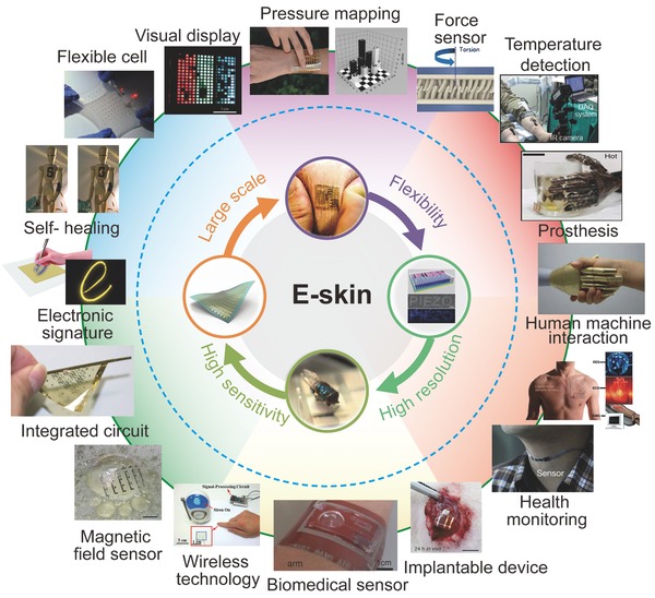
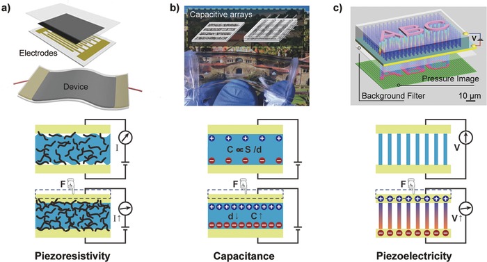
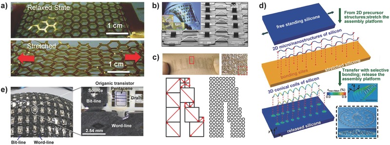
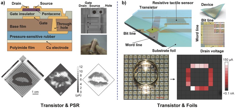
The skin is the largest organ of the human body and can sense pressure, temperature, and other complex environmental stimuli or conditions. The mimicry of human skin's sensory ability via electronics is a topic of innovative research that could find broad applications in robotics, artificial intelligence, and human-machine interfaces, all of which promote the development of electronic skin (e-skin). To imitate tactile sensing via e-skins, flexible and stretchable pressure sensor arrays are constructed based on different transduction mechanisms and structural designs. These arrays can map pressure with high resolution and rapid response beyond that of human perception. Multi-modal force sensing, temperature, and humidity detection, as well as self-healing abilities are also exploited for multi-functional e-skins. Other recent progress in this field includes the integration with high-density flexible circuits for signal processing, the combination with wireless technology for convenient sensing and energy/data transfer, and the development of self-powered e-skins. Future opportunities lie in the fabrication of highly intelligent e-skins that can sense and respond to variations in the external environment. The rapidly increasing innovations in this area will be important to the scientific community and to the future of human life.

Keywords: electronic skin; flexible; multifunctional device; pressure mapping; tactile sensor.


Figures

Figure 1
Figure 1
Characteristic properties and diverse functions or applications of recently developed devices for e‐skins. “Large scale:” Reproduced with permission.12 Copyright 2013, Macmillan Publishers Ltd. “High sensitivity:” Reproduced with permission.31 Copyright 2010, Macmillan Publishers Ltd. “High resolution:” Reproduced with permission.[[qv: 15a]] Copyright 2013, Macmillan Publishers Ltd. "Pressure mapping:” Reproduced with permission.[[qv: 13b]] Copyright 2014, Macmillan Publishers Ltd. Reproduced with permission.30 Copyright 2015, Macmillan Publishers Ltd. “Force sensor:” Reproduced with permission.10 Copyright 2012, Macmillan Publishers Ltd. “Prosthesis:” Reproduced with permission.[[qv: 9b]] Copyright 2014, Macmillan Publishers Ltd. “Magnetic field sensor:” Reproduced with permission.106 Copyright 2015, Macmillan Publishers Ltd. “Integrated circuit:” Reproduced with permission.105 Copyright 2008, American Association for the Advancement of Science. “Self‐healing:” Reproduced with permission.[[qv: 11a]] Copyright 2012, Macmillan Publishers Ltd. “Flexible cell:” Reproduced with permission.75 Copyright 2013, Macmillan Publishers Ltd. “Visual display:” Reproduced with permission.61 Copyright 2013, Macmillan Publishers Ltd. “Health monitoring:” Reproduced with permission.[[qv: 1c]] Copyright 2014, Royal Society of Chemistry. Reproduced with permission.19 Copyright 2014, Macmillan Publishers Ltd. “Temperature detection:” Reproduced with permission.96 “Biomedical sensor:” Reproduced with permission.111 “Implantable device:” Reproduced with permission.[[qv: 107a]] “Electronic signature:” Reproduced with permission.74 “Flexibility:” Reproduced with permission.[[qv: 9a]] Copyright 2011, American Association for the Advancement of Science. “Wireless technology:” Reproduced with permission.82 Copyright 2014, American Chemical Society. “Human machine interaction:” Reproduced with permission.[[qv: 1g]] Copyright 2012, Cambridge University Press.
Figure 2
Figure 2
Schematic illustrations of three common transduction methods and representative devices: a) piezoresistivity, b) capacitance, and c) piezoelectricity. Reproduced with permission.[[qv: 15a]],21, 29 Copyright 2013, 2014, and 2011, respectively, Macmillan Publishers Ltd.
Figure 3
Figure 3
Different strategies to achieve stretchability. a) Net‐shaped structural design. Reproduced with permission.[[qv: 41b]] Copyright 2011, American Chemical Society. b) Noncoplanar mesh design. Reproduced with permission.44 Copyright 2008, National Academy of Sciences. c) Fractal design. Reproduced with permission.45 Copyright 2014, Macmillan Publishers Ltd. d) 3D architectures via compressive buckling. Reproduced with permission.47 Copyright 2015, American Association for the Advancement of Science. e) Use of elastic conductors. Reproduced with permission.49 Copyright 2008, American Association for the Advancement of Science.
Figure 4
Figure 4
Two typical structure diagrams of pressure‐sensitive transistor active matrix sensors based on the piezoresistive transduction methods. a) Transistor array laminated with a pressure‐sensitive rubber layer. Reproduced with permission.23 Copyright 2004, National Academy of Sciences. b) Transistor array integrated with resistive tactile sensing foils. Reproduced with permission.12 Copyright 2013, Macmillan Publishers Ltd.
Figure 5
Figure 5
Transistor active matrix sensors for pressure mapping. a) Ge/Si nanowire‐array FETs integrated with a PSR sheet. Reproduced with permission.57 Copyright 2010, Macmillan Publishers Ltd. b) Carbon nanotube TFTs integrated with a PSR layer and OLEDs to achieve pressure visualization. Reproduced with permission.61 Copyright 2013, Macmillan Publishers Ltd.
Figure 6
Figure 6
Highly sensitive active matrix sensors with geometric design of gate dielectric. a) Pressure‐sensitive OFET with microstructured PDMS dielectric layer. b) Flexible pixel‐type capacitive pressure sensor array using a microstructured PDMS film as a dielectric layer. c) Pressure response curves of the capacitive sensors fabricated with different types of microstructured PDMS films. d) Change in I DS of the OFET in response to pressure, which is proportional to the change in relative capacitive and exhibits a rapid response. Reproduced with permission.31 Copyright 2010, Macmillan Publishers Ltd. e) Flexible active matrix with high‐pressure sensitivity and a microstructured dielectric layer. f) 2D pressure imaging using a transistor active matrix. Reproduced with permission.62 Copyright 2013, Macmillan Publishers Ltd.
Figure 7
Figure 7
Pressure mapping based on piezotronics. a) Schematic structure of a 3D strain‐gated vertical piezotronic transistor matrix. The color gradient in the enlarged view inset illustrates the piezopotential field induced by the applied force, in which red and blue, respectively, represent positive and negative piezopotentials. b) Origins of piezotronics, piezo‐phototronics, and piezophotonics, which provide the coupling between/among the semiconductor, piezoelectricity, and photoexcitation. c) Current response of a piezotronic transistor to applied pressure. d) Statistical current distribution of the integrated transistor array without applied pressure. e) Current distribution of the array under pressure. Reproduced with permission.[[qv: 15b]] Copyright 2013, American Association for the Advancement of Science.
Figure 8
Figure 8
Pressure mapping based on piezo‐phototronics. a) Schematic structure of the nanowire‐LED‐based pressure sensor array. b) Change in emission enhancement of an LED pixel in response to strain. c) Measured response time of the device is ≈90 ms. d) Spatial resolution of the array is estimated as 2.7 μm. e) Photograph of a electroluminescent device under a bias voltage of 5 V. f) High‐resolution pressure imaging. Reproduced with permission.[[qv: 15a]] Copyright 2013, Macmillan Publishers Ltd.
Figure 9
Figure 9
Flexible piezo‐phototronic nanowire LED array for pressure mapping. a) Schematic illustration and photograph of the flexible device. b) Electron band diagram showing the piezo‐phototropic effect. c) Pressure mapping result. d) Light intensity enhancement as a function of the area of ZnO NWs. Reproduced with permission.[[qv: 73a]]
Figure 10
Figure 10
Pressure mapping based on piezophotonics. a) Schematic structure of the device. b) Band diagram of ZnS:Mn, which indicates the action mechanism of piezophotonic effect. c) Dynamic pressure mapping of 2D planar and single‐point models. d) Signature recording and high‐resolution pressure mapping. Reproduced with permission.74
Figure 11
Figure 11
Developments in self‐powered pressure‐sensitive triboelectric sensors. a) First flexible triboelectric self‐powered pressure sensor. Reproduced with permission.81 Copyright 2012, American Chemical Society. b) Self‐powered ultra‐sensitive flexible tactile sensor. Reproduced with permission.82 Copyright 2014, American Chemical Society. c) Stretchable tactile sensor that can differentiate multiple mechanical stimuli and could be self‐powered. Reproduced with permission.83
Figure 12
Figure 12
Integrated self‐powered triboelectric sensor array capable of mapping applied pressure. a) Structural illustration of a single triboelectric sensor with a photograph of the device as the inset. b) Schematic illustration of an integrated triboelectric sensor array. c) The 2D output voltage contour plots from the sensor matrix under external pressure applied through architectures with designed calligraphy. Reproduced with permission.84 Copyright 2013, American Chemical Society.
Figure 13
Figure 13
Self‐powered single‐electrode‐based triboelectric sensor array that can track the motion trajectory of an object. a) Schematic diagram of the device and its working process of the sensor array. b) Finite element simulation of the potential distribution on the array when a ball moves on the surface of the PTFE film. c) Motion imaging result of an Al ball moving on the sensor array along a specific path. Reproduced with permission.86
Figure 14
Figure 14
Self‐healing pressure sensor for e‐skin. a) Electrical healing process recorded by the time evolution of measured resistance. Inset: Optical images of damaged and self‐healed samples (upper) and proposed interaction of oligomer chains with Ni particles (lower). b) Demonstration of the self‐healing process of a conductive composite using a LED. c) Circuit diagram and photograph of a self‐healing tactile sensor mounted on a doll. d) Demonstration of self‐healing process in electrical and mechanical characterization. Reproduced with permission.[[qv: 11a]] Copyright 2012, Macmillan Publishers Ltd.
Figure 15
Figure 15
Bio‐inspired design for multi‐force sensing. a) Hair‐to‐hair interlock inspired highly sensitive strain sensor using reversible interlocking of nanofibers. Reproduced with permission.10 Copyright 2012, Macmillan Publishers Ltd. b) Whisker inspired wind sensing e‐whiskers. Reproduced with permission.92 Copyright 2012, National Academy of Sciences. c) Spider‐sensory‐system‐inspired crack‐based strain and vibration sensor. Reproduced with permission.19 Copyright 2014, Macmillan Publishers Ltd.
Figure 16
Figure 16
Flexible temperature‐ and pressure‐sensitive sensors. a) Multifunctional epidermal electronic system attached on skin: undeformed (left), crinkled (middle), and stretched (right) states. Reproduced with permission.[[qv: 9a]] Copyright 2011, American Association for the Advancement of Science. b) Ultrathin conformal temperature sensor arrays based on TCR materials and PIN diodes. Reproduced with permission.95 Copyright 2013, Macmillan Publishers Ltd. c) Flexible pressure and temperature sensor array based on organic transistors. Reproduced with permission.99 Copyright 2005, National Academy of Sciences.
Figure 17
Figure 17
Multi‐functionalized prosthesis with stretchable e‐skin that can sense pressure, temperature, and humidity and can serve as electro‐resistive heaters and stretchable multi‐electrode arrays. a) Photograph of the prosthesis. b) Layered structure of the e‐skin. c) Practical applications of the prosthesis. Reproduced with permission.[[qv: 9b]] Copyright 2014, Macmillan Publishers Ltd.
Figure 18
Figure 18
Highly integrated e‐skin systems. a) Stretchable and foldable silicon integrated circuits for e‐skin. Reproduced with permission.104 Copyright 2008, American Association for the Advancement of Science. b) Functional organic TFTs and circuits on a flexible ultrathin polymide substrate. Reproduced with permission.105 Copyright 2010, Macmillan Publishers Ltd. c) Ultra‐lightweight electronics on ultrathin flexible polymer foil that can sense magnetic fields based on giant magnetoresistance effect. Reproduced with permission.106 Copyright 2015, Macmillan Publishers Ltd.
Figure 19
Figure 19
Applications of wireless technology on e‐skin. a) Flexible wireless pressure sensor array. Reproduced with permission.[[qv: 16c]] Copyright 2014, Macmillan Publishers Ltd. b) Wireless energy‐transfer module for e‐skin. Reproduced with permission.46 Copyright 2014, American Association for the Advancement of Science. c) Touch and temperature sensor array integrated with wireless data transmission module. Reproduced with permission.111

Similar articles

Cited by

References

    1. a) Maheshwari V., Saraf R. F., Angew. Chem., Int. Ed. 2008, 47, 7808; - PubMed
    2. b) Hammock M. L., Chortos A., Tee B. C. K., Tok J. B. H., Bao Z., Adv. Mater. 2013, 25, 5997; - PubMed
    3. c) Guo C., Yu Y., Liu J., J. Mater. Chem. B 2014, 2, 5739; - PubMed
    4. d) Jung S., Kim J. H., Kim J., Choi S., Lee J., Park I., Hyeon T., Kim D.‐H., Adv. Mater. 2014, 26, 4825; - PubMed
    5. e) Lee J., Kim S., Lee J., Yang D., Park B. C., Ryu S., Park I., Nanoscale 2014, 6, 11932; - PubMed
    6. f) Wang X.‐Q., Wang C.‐F., Zhou Z.‐F., Chen S., Adv. Opt. Mater. 2014, 2, 652;
    7. g) Sekitani T., Someya T., Mrs Bull. 2012, 37, 236.
    1. a) Engel J., Chen J., Fan Z. F., Chang L., Sens. Actuators A 2005, 117, 50;
    2. b) Hou C., Wang H., Zhang Q., Li Y., Zhu M., Adv. Mater. 2014, 26, 5018; - PubMed
    3. c) Wang X., Gu Y., Xiong Z., Cui Z., Zhang T., Adv. Mater. 2014, 26, 1336; - PubMed
    4. d) Chortos A., Bao Z. N., Mater. Today 2014, 17, 321.
    1. a) Bauer S., Bauer‐Gogonea S., Graz I., Kaltenbrunner M., Keplinger C., Schwodiauer R., Adv. Mater. 2014, 26, 149; - PMC - PubMed
    2. b) Silvera‐Tawil D., Rye D., Soleimani M., Velonaki M., IEEE Sens. J. 2015, 15, 2001.
    1. a) Clippinger F. W., Avery R., Titus B. R., Bull. Prosthetics Res. 1974, 247; - PubMed
    2. b) Vedel J. P., Roll J. P., Neurosci. Lett. 1982, 34, 289. - PubMed
    1. a) Jiang F. K., Tai Y. C., Walsh K., Tsao T., Lee G. B., Ho C. M., in Proc. IEEE Tenth Annu. Int. Workshop on Micro. Electro. Mech. Syst., Nagoya, Japan: 1997, 465;
    2. b) Lacour S. P., Wagner S., Huang Z. Y., Suo Z., Appl. Phys. Lett. 2003, 82, 2404.