Review
. 2017 Jan 31;17(3):362-381.
doi: 10.1039/c6lc01173j.

Thermoplastic nanofluidic devices for biomedical applications

Affiliations
Review

Thermoplastic nanofluidic devices for biomedical applications

Kumuditha M Weerakoon-Ratnayake et al. Lab Chip. .

Abstract

Microfluidics is now moving into a developmental stage where basic discoveries are being transitioned into the commercial sector so that these discoveries can affect, for example, healthcare. Thus, high production rate microfabrication technologies, such as thermal embossing and/or injection molding, are being used to produce low-cost consumables appropriate for commercial applications. Based on recent reports, it is clear that nanofluidics offers some attractive process capabilities that may provide unique venues for biomolecular analyses that cannot be realized at the microscale. Thus, it would be attractive to consider early in the developmental cycle of nanofluidics production pipelines that can generate devices possessing sub-150 nm dimensions in a high production mode and at low-cost to accommodate the commercialization of this exciting technology. Recently, functional sub-150 nm thermoplastic nanofluidic devices have been reported that can provide high process yield rates, which can enable commercial translation of nanofluidics. This review presents an overview of recent advancements in the fabrication, assembly, surface modification and the characterization of thermoplastic nanofluidic devices. Also, several examples in which nanoscale phenomena have been exploited for the analysis of biomolecules are highlighted. Lastly, some general conclusions and future outlooks are presented.


Figures

Figure 1
Figure 1
Required pressure drop and voltage drop for nanochannels with different channel heights. Nanochannel length and width are 3.5 μm and 2.3 μm, respectively; zeta potential is −11 mV for 1 M NaCl solution. Reproduced from Conlisk et al. ELECTROPHORESIS, 2005, 26, 1896–1912. Insert shows the comparison between the parabolic and plug flow profiles from the pressure-driven and electroosmotic flow, respectively.
Figure 2
Figure 2
(A) A schematic of the design and fabrication process of a thermoplastic-based nanofluidic device. (a) Silicon master, which consisted of micron-scale transport channels, nanochannels and a funnel-like inlet for the nanochannels; (b)-(d) fabrication steps to produce a protrusive polymer stamp in a UV-curable resin by imprinting from the silicon master; (e)-(g) fabrication steps to generate nanofluidic structures in PMMA by imprinting from the UV-curable resin stamp; (h) bonding step with a PMMA cover plate to build the enclosed mixed-scale polymer device with microchannels and nanochannels. (B) (a) Schematic of the protocol used for assembly of a hybrid fluidic device and the thermal press instrument. (b) Temperature-pressure process profile showing the six stages for the thermal fusion bonding cycle. See main text for a description of the 6 stages of bonding. Reproduced from Wu et al. Lab on a Chip, 2011, 11, 2984–2989 and Uba et al. Lab on a Chip, 2015, 15, 1038–1049 (with permission from The Royal Society of Chemistry).
Figure 3
Figure 3
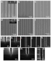
SEMs of Si masters (a, d, g, h, i, l, m), resin stamps (b, e, j) and nanofluidic devices imprinted in PMMA (c, f, k, n). The device in a – c is a nanoslit device with a width of 1 μm and depth of 50 nm. In d – f, a device with a 120 nm × 120 nm channel is shown. In g – k, a nanofluidic device with 40 × 40 nm channel is shown with a 40 nm thick Al layer that was deposited onto the Si master prior to focused ion beam milling, which was used to generate the nano-structures. In l – n is shown a nanofluidic device with an approximate 20 × 20 nm channel with a 80 nm thick Al layer deposited onto the Si master prior to focused ion beam milling. In all cases, the substrate used was PMMA (glass transition temperature = 105°C). Figures a – f, m – n were reproduced with permission of The Royal Society of Chemistry from Uba et al. Analyst, 2014, 139. Figures g – k and l are unpublished.
Figure 4
Figure 4
(A) (a) Graphs showing the average extension length (Lav) of 10 different T4 DNA molecules. Lav has been measured 100, 250 and 400 μm from the nanochannel entrance for each molecule. The inset shows a typical intensity time-trace of a T4 molecule confined inside a PMMA nanochannel. The scale bar is 10 μm and the time span is 50 s. (b) Histogram of the measured extension lengths (Lext) of DNA molecule 2 positioned 100 μm from the nanochannel entrance. The average extension length, based on an analysis of 500 consecutive frames, Lav = 13.4 μm and the standard deviation σav = 1.0 μm. The dashed line shows the Gaussian curve fit. (c) Histogram of the measured average extension lengths of Lav presented in (a). The overall average Lav was 13.5 μm with a standard deviation of 0.5 μm. Reprinted from Thamdrup et al., Nanotechnology, 2008, 19, 125301 with permission from IOP Publishing. (B) (a) SEM micrograph of a nickel plate with an array of 240 nm wide and 150 nm high protrusions. (b) Corresponding nanochannel array injection molded in Topas 5013. To avoid charging effects during SEM imaging, the chip surface was sputtered with 5 nm of gold. (c) Three dimensional AFM image of a channel segment, taken for the same array as in (b). Adapted from Utko et al., Lab on a Chip, 2011, 11, 303–308 with permission of The Royal Society of Chemistry
Figure 5
Figure 5
(A) Unprocessed representative frames of T4 DNA molecules elongated in enclosed hybrid-based nanochannel devices. Images were acquired at 10 ms exposure time with the driving field turned-off. Note that nc6 = 35 × 35 nm. (B) Log-log plot showing T4 DNA extension as a function of the geometric average depth of the nanochannels. The DNA extension was normalized to a total contour length (Lc) of 64 μm for the dye-labeled molecules. The red and blue dashed lines are the deGennes and Odijk predictions, respectively. The black solid line is the best power-law fit to the data points obtained from the nanochannels with an average geometric depth range of 53 nm to 200 nm. Reproduced from Uba et al., Lab on a Chip, 2015, 15, 1038–1049 with permission from The Royal Society of Chemistry
Figure 6
Figure 6
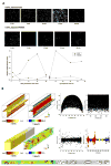
(A) Representative STORM images of 1 μm2 (a–e) COC and (f–j) PMMA exposed to 1, 5, 10, 15, and 20 min UV/O3 radiation, respectively. Relative –COOH density vs exposure time for (k) UV/O3 and (l) O2 plasma-modified COC (closed squares) and PMMA (open circles). Lines are for visual purposes only. UV/O3 and O2 plasma exposure conditions were kept constant. All total localizations were normalized to the greatest localization density, which was for COC exposed to 10 s of O2 plasma. (B) (a) COMSOL simulation showing the electric potential (left) and velocity magnitude (right) for a channel with uniform surface charge; (b) Velocity vs axial (right) and longitudinal (left) position to show the EOF flow profile for a channel with uniform surface charge; (c) One slice of the velocity magnitude of a uniform channel; (d) Streamline of the same velocity slice depicted in (c); (e) COMSOL simulation showing the electric potential (left) and velocity magnitude (right) where single point charges were mapped onto the nanochannel surfaces using the –COOH locations (centroids) obtained by STORM analysis of a COC surface exposed to 5 min UV/O3 activation. (f) Velocity vs axial (right) and longitudinal (left) position to show the EOF flow profile for the channel with non-uniform surface charge. The colors in the velocity vs Z position graph (right) represent an area in the channel with >5 (red), 3–4 (blue), and 1–2 (yellow) –COOH group(s) within 20 nm of each other. (g) One slice of the velocity profile to show fluid flow recirculation. (h) Streamline of the same velocity slice depicted in (e) to emphasize the fluid recirculation at areas with –COOH. Reprinted with permission from O’Neil et al., Analytical Chemistry, 2016, 88, 3686–3696 (American Chemical Society).
Figure 7
Figure 7
(A) Schematic of the dark field microscope and the experimental setup. The sample was mounted on a level-controlled microscope stage. While the spider stop controlled white light missed the objective, only scattered light from the sample entered the objective. (B) Image of the PMMA nanofluidic chip and a schematic of the device with nanoslits. (C) Schematic of the nanoslits when an external electric field was applied. Electroosmotic flow was from anode to cathode while the electrophoretic mobility of negatively charged AgNPs was toward the anode. (D) Representation of a translocation event for a 60 nm AgNP in a nanoslit. Time-lapse image sequence of the single AgNP event with an external field strength = 200 V/cm. The particle translocation direction was from anode to cathode (same direction as EOF) with a translocation time of 1.3 s. Dimensions of the nanoslits were 100 μm in length and 150 nm deep. Histograms of translocation events for 60 nm AgNPs (blue) and 100 nm AgNPs (red) in 150 nm nanoslits with a running buffer of 0.05 mM citrate. Each histogram includes 100 events at a bias voltage of (E) 100 V/cm, (F) 200 V/cm, (G) 500 V/cm, and (H) 1500 V/cm. Note that the time axes have different scales depending on the electric field. Weerakoon Ratnayake et al., Analytical Chemistry, 2016, 88, 3569–3577 (American Chemical Society).
Figure 8
Figure 8
(A) Representative schematic of λ exonuclease immobilized onto a PMMA pillar as it processively cleaves dNMPs from a double stranded (ds) DNA molecule. Fluorescence images showing the digestion of dsDNA by λ exonuclease immobilized onto a PMMA pillar. Oliver-Calixte et al., Analytical Chemistry, 2014, 86, 4447–4454 (ACS Author’s Choice article, American Chemical Society). (B) Molecular dynamic simulations of the translocation of single dNMP molecules within nanochannels showing the separation of dCMP, dGMP, dAMP and dTMP (Novak et al., Journal of Physical Chemistry B, 2013, 117, 3271–3279, American Chemical Society).
Figure 9
Figure 9
(A) Schematic illustration for SNP detection based on molecular recognition using DNA-functionalized nanochannels (Yang et al., Nano Letters, 2011, 11, 1032–1035, American Chemical Society). (B) Schematic layout of a nanofluidics chip. Green and pink colors denote enzyme and substrate, respectively; yellow denotes the reaction product. The product of the enzymatic reaction, hydrogen peroxide, was electrochemically determined as indicated by the rise of the current when the substrate, glucose, was introduced. The working electrode was aligned to the end of the nanochannel with a distance of 20 mm. Reproduced from Wang et al., Lab on a Chip, 2013, 13, 1546–1553 (The Royal Society of Chemistry).

Similar articles

Cited by

References

    1. Kim SJ, Wang YC, Lee JH, Jang H, Han J. Physical Review Letters. 2007;99:044501. - PMC - PubMed
    1. Anand RK, Sheridan E, Knust KN, Crooks RM. Analytical Chemistry. 2011;83:2351–2358. - PubMed
    1. Mani A, Zangle TA, Santiago JG. Langmuir. 2009;25:3898–3908. - PMC - PubMed
    1. Piruska A, Gong M, Sweedler JV, Bohn PW. Chemical Society Reviews. 2010;39:1060–1072. - PubMed
    1. Zangle TA, Mani A, Santiago JG. Chemical Society Reviews. 2010;39:1014–1035. - PubMed

Publication types

MeSH terms

LinkOut - more resources