. 2017 Jan 10;114(2):233-238.
doi: 10.1073/pnas.1617186114. Epub 2016 Dec 27.

Transparent amorphous oxide semiconductors for organic electronics: Application to inverted OLEDs

Affiliations

Transparent amorphous oxide semiconductors for organic electronics: Application to inverted OLEDs

Hideo Hosono et al. Proc Natl Acad Sci U S A. .

Abstract

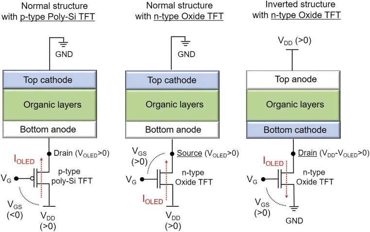
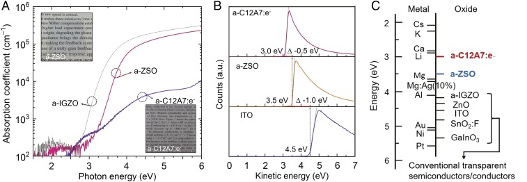
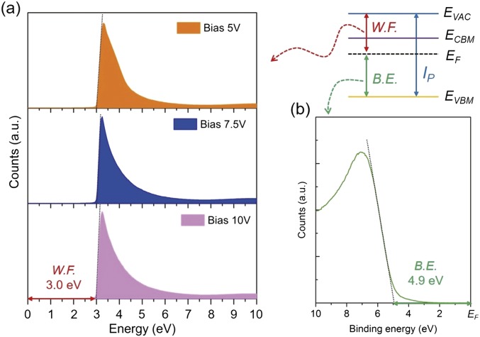
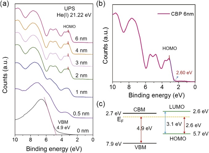
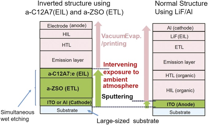
Efficient electron transfer between a cathode and an active organic layer is one key to realizing high-performance organic devices, which require electron injection/transport materials with very low work functions. We developed two wide-bandgap amorphous (a-) oxide semiconductors, a-calcium aluminate electride (a-C12A7:e) and a-zinc silicate (a-ZSO). A-ZSO exhibits a low work function of 3.5 eV and high electron mobility of 1 cm2/(V · s); furthermore, it also forms an ohmic contact with not only conventional cathode materials but also anode materials. A-C12A7:e has an exceptionally low work function of 3.0 eV and is used to enhance the electron injection property from a-ZSO to an emission layer. The inverted electron-only and organic light-emitting diode (OLED) devices fabricated with these two materials exhibit excellent performance compared with the normal type with LiF/Al. This approach provides a solution to the problem of fabricating oxide thin-film transistor-driven OLEDs with both large size and high stability.

Keywords: amorphous oxide semiconductor; electron injection; electron transport; inverted OLEDs; low work function material.


Conflict of interest statement

The authors declare no conflict of interest.

Figures

Fig. 1.
Fig. 1.
Circuits and applied voltages in two types of OLED device structures and driving TFTs with different polarity. Current through OLED (IOLED) is given by IOLED ∝ (VGS – Vth)2 in a saturation region, where VGS and Vth denote the voltage biasing between gate and source and the threshold voltage, respectively. Here VGS = VG – (VDD + VOLED) for n-channel TFTs with normal structure but VGS = VG – VD for p-channel TFTs with normal OLED structure and n-channel TFTs with inverted structure, where VG, VD, and VOLED are gate voltage, drain voltage, and voltage through the OLED, respectively. The variation in the electrical properties of OLED devices, which are sensitive to aging and so on, directly leads to the variation in IOLED, that is, luminous intensity, through the change in VGS. This is why the inverted OLED structure is favorable for being driven by n-channel TFTs with an oxide semiconductor as the active layer.
Fig. 2.
Fig. 2.
Physical properties of amorphous C12A7:e and ZSO thin films deposited on SiO2 glass substrates by sputtering at RT. (A) Optical absorption spectra and photographs of the thin films. The sample thicknesses are ∼200 nm. A-ZSO is more transparent than a-IGZO for oxide TFTs. (B) Secondary electron emission cutoff spectra measured by UV photoemission spectroscopy (UPS) along with that of ITO for comparison, and (C) work function values of various metals and transparent oxide semiconductors. Mg:Ag(10%) is practically used as the cathode with a combination of a very thin LiF layer such as LiF/Al (29).
Fig. S1.
Fig. S1.
UPS spectra of a-C12A7:e thin films. The work function of 3.0 eV was determined from the bias independent secondary electron cutoff (A). The valence band maximum energy was determined to be 4.9 eV from the Fermi level (B). The ionization energy (7.9 eV) is the sum of work function (3.0 eV) and the valence band maximum energy (4.9 eV).
Fig. S2.
Fig. S2.
(A) UPS spectra of CBP deposited on a-C12A7:e. (B) Zoomed-in view of the spectrum near the Fermi level. (C) Energy level diagram of a-C12A7:e and CBP. CBM and VBM denote the valence band maximum and conduction band minimum, respectively.
Fig. S3.
Fig. S3.
Current–voltage characteristics of the contacts between a cathode metal (Al) and a-ZSO with different resistivities controlled by partial oxygen pressure during deposition (A) or postannealing temperature (B). The resistivity of a-ZSO thin films is adjusted by varying oxygen partial pressure (0.1–1%) during deposition. Ohmic contacts are realized over a wide range of voltages for both metals except an a-ZSO sample with extremely high resistivity that was deposited under the highest PO2 atmosphere.
Fig. 3.
Fig. 3.
Energy diagram of an inverted OLED device using a-C12A7:e (EIL) and a-ZSO (ETL). The values of the ionization energy (Ip) were determined from the location of the valence band measured by UPS as shown in Figs. S1 and S2. MoOx and NPD, N,N′-di(1-naphthyl)-N,N′-diphenyl- (1,1′-biphenyl)-4,4′-diamine, are used as hole injection layer (HIL) and HTL, respectively, and CBP doped with Ir(ppy)3, tris[2-phenylpyridinato-C2,N]iridium(III), is used as the EML. Note that the stacking order of injection layer and transport layer for electrons is reversed for the hole. This sequence for the electron is designed to use the ohmic contact between a-ZSO and the cathode materials.
Fig. 4.
Fig. 4.
Comparison of the performance of OLEDs with different stacking structures and different EIL and ETL materials. (A) Current–voltage characteristics of electron-only devices. Alq3 and BCP are used as the electron transport material and hole-blocking material, respectively. (Right) Device stacking structure. (B) Luminous intensity vs. voltage characteristics of OLEDs. (Right) Device stacking structure. (C) The dependence of the luminous characteristics on the ETL thickness. Three thicknesses are chosen to correspond to the calculated optimal values for light extraction from the inverted top emission device. (D) Current efficiency vs. luminance for inverted and normal-type devices. Note that the devices used for this measurement are not the same as those for C but were fabricated by the same procedures as those for C.
Fig. S4.
Fig. S4.
Log J-V1/2 plots for data on electron-only devices data in Fig. 4A.
Fig. S5.
Fig. S5.
Proposed process for efficient production of large-sized OLEDs using a-C12A7:e and a-ZSO. The bottom three layers can be deposited by sputtering just as in the practical LCD fabrication process. The resulting multilayer thin films are taken out from the vacuum chamber and then followed by nonvacuum processes used in conventional OLED fabrication shown on the right.
Fig. S6.
Fig. S6.
Photograph of a sputtering target of c-C12A7:e. The dense sintered targets up to 6 in. in diameter are available.

References

    1. Katz HE, Huang J. Thin-film organic electronic devices. Annu Rev Mater Res. 2009;39:71–92.
    1. Gärtner C, et al. The influence of annihilation processes on the threshold current density of organic laser diodes. J Appl Phys. 2007;101(2):023107.
    1. Gong X, et al. Bulk heterojunction solar cells with large open-circuit voltage: Electron transfer with small donor-acceptor energy offset. Adv Mater. 2011;23(20):2272–2277. - PubMed
    1. Ma R. Organic Electroluminescent Displays. In: Chen J, Cranton W, Fihn M, editors. Handbook of Visual Display Technology. Vol. 2. Springer; Berlin: 2012. pp. 1210–1237.
    1. Chen CW, Lin CL, Wu CC. An effective cathode structure for inverted top-emitting organic light-emitting devices. Appl Phys Lett. 2004;85(13):2469–2471.

Publication types