Origins and demonstrations of electrons with orbital angular momentum
- PMID: 28069765
- PMCID: PMC5247478
- DOI: 10.1098/rsta.2015.0434
Origins and demonstrations of electrons with orbital angular momentum
Abstract
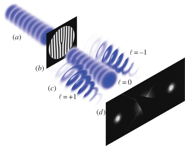
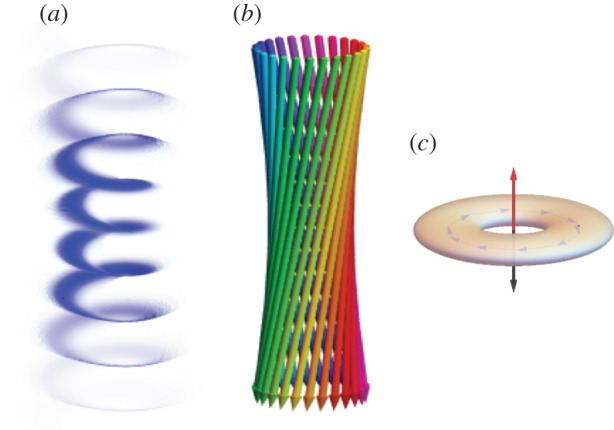
The surprising message of Allen et al. (Allen et al. 1992 Phys. Rev. A 45, 8185 (doi:10.1103/PhysRevA.45.8185)) was that photons could possess orbital angular momentum in free space, which subsequently launched advancements in optical manipulation, microscopy, quantum optics, communications, many more fields. It has recently been shown that this result also applies to quantum mechanical wave functions describing massive particles (matter waves). This article discusses how electron wave functions can be imprinted with quantized phase vortices in analogous ways to twisted light, demonstrating that charged particles with non-zero rest mass can possess orbital angular momentum in free space. With Allen et al. as a bridge, connections are made between this recent work in electron vortex wave functions and much earlier works, extending a 175 year old tradition in matter wave vortices.This article is part of the themed issue 'Optical orbital angular momentum'.
Keywords: electron vortex; matter wave interferometry; optical angular momentum.
© 2017 The Author(s).
Figures
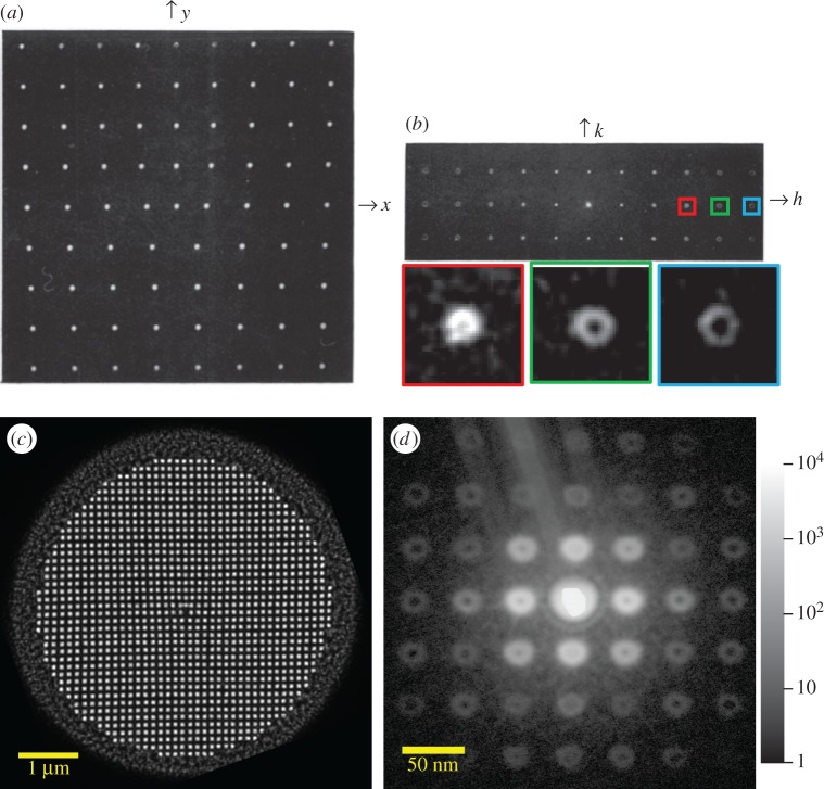
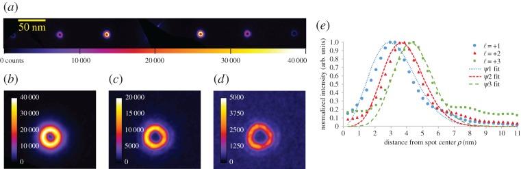
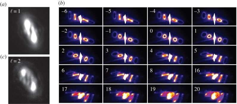
 units of OAM.
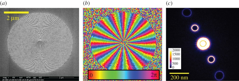
 are visible. Such beams are very sensitive to imperfections in the electron optics, and any small leftover astigmatism results in elliptic distortions seen here.
Similar articles
-
Optical orbital angular momentum.Philos Trans A Math Phys Eng Sci. 2017 Feb 28;375(2087):20150444. doi: 10.1098/rsta.2015.0444. Philos Trans A Math Phys Eng Sci. 2017. PMID: 28069775 Free PMC article.
-
Orbital angular momentum of single photons: revealing quantum fundamentals.Philos Trans A Math Phys Eng Sci. 2024 Dec 30;382(2287):20230327. doi: 10.1098/rsta.2023.0327. Epub 2024 Dec 24. Philos Trans A Math Phys Eng Sci. 2024. PMID: 39717988 Free PMC article. Review.
-
Optical angular momentum and atoms.Philos Trans A Math Phys Eng Sci. 2017 Feb 28;375(2087):20150435. doi: 10.1098/rsta.2015.0435. Philos Trans A Math Phys Eng Sci. 2017. PMID: 28069766 Free PMC article. Review.
-
Analogies between optical and quantum mechanical angular momentum.Philos Trans A Math Phys Eng Sci. 2017 Feb 28;375(2087):20150443. doi: 10.1098/rsta.2015.0443. Philos Trans A Math Phys Eng Sci. 2017. PMID: 28069774
-
Direct Mechanical Detection and Measurement of Wave-Matter Orbital Angular Momentum Transfer by Nondissipative Vortex Mode Conversion.Phys Rev Lett. 2019 Dec 13;123(24):244301. doi: 10.1103/PhysRevLett.123.244301. Phys Rev Lett. 2019. PMID: 31922856
Cited by
-
Demonstration of angular-momentum-resolved electron energy-loss spectroscopy.Nat Commun. 2025 Jul 17;16(1):6601. doi: 10.1038/s41467-025-60804-3. Nat Commun. 2025. PMID: 40675985 Free PMC article.
-
SU(N) symmetry of coherent photons controlled by rotated waveplates.Heliyon. 2024 Jul 14;10(14):e34423. doi: 10.1016/j.heliyon.2024.e34423. eCollection 2024 Jul 30. Heliyon. 2024. PMID: 39114062 Free PMC article.
-
Optical orbital angular momentum.Philos Trans A Math Phys Eng Sci. 2017 Feb 28;375(2087):20150444. doi: 10.1098/rsta.2015.0444. Philos Trans A Math Phys Eng Sci. 2017. PMID: 28069775 Free PMC article.
-
Conservation laws for electron vortices in strong-field ionisation.Eur Phys J D At Mol Opt Phys. 2021;75(7):199. doi: 10.1140/epjd/s10053-021-00214-4. Epub 2021 Jul 9. Eur Phys J D At Mol Opt Phys. 2021. PMID: 34720728 Free PMC article.
-
Multiplication and division of the orbital angular momentum of light with diffractive transformation optics.Light Sci Appl. 2019 Dec 5;8:113. doi: 10.1038/s41377-019-0222-2. eCollection 2019. Light Sci Appl. 2019. PMID: 31814970 Free PMC article.
References
-
- Whewell W. 1833. Essay towards a first approximation to a map of cotidal lines. Phil. Trans. R. Soc. Lond. 123, 147–236. (10.1098/rstl.1833.0013) - DOI
-
- Whewell W. 1836. On the results of an extensive system of tide observations made on the coasts of Europe and America in June 1835. Phil. Trans. R. Soc. Lond. 126, 289–341. (10.1098/rstl.1836.0019) - DOI
-
- Berry MV. 1981. Singularities in waves and rays. In Lecture series session, no. 35 (ed. Les Houches), pp. 453–543. Amsterdam, The Netherlands: North-Holland.
LinkOut - more resources
Full Text Sources
Other Literature Sources