. 2017 Jan 23:8:14243.
doi: 10.1038/ncomms14243.

Wafer-scale integration of sacrificial nanofluidic chips for detecting and manipulating single DNA molecules

Affiliations

Wafer-scale integration of sacrificial nanofluidic chips for detecting and manipulating single DNA molecules

Chao Wang et al. Nat Commun. .

Abstract

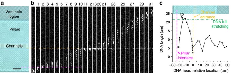
Wafer-scale fabrication of complex nanofluidic systems with integrated electronics is essential to realizing ubiquitous, compact, reliable, high-sensitivity and low-cost biomolecular sensors. Here we report a scalable fabrication strategy capable of producing nanofluidic chips with complex designs and down to single-digit nanometre dimensions over 200 mm wafer scale. Compatible with semiconductor industry standard complementary metal-oxide semiconductor logic circuit fabrication processes, this strategy extracts a patterned sacrificial silicon layer through hundreds of millions of nanoscale vent holes on each chip by gas-phase Xenon difluoride etching. Using single-molecule fluorescence imaging, we demonstrate these sacrificial nanofluidic chips can function to controllably and completely stretch lambda DNA in a two-dimensional nanofluidic network comprising channels and pillars. The flexible nanofluidic structure design, wafer-scale fabrication, single-digit nanometre channels, reliable fluidic sealing and low thermal budget make our strategy a potentially universal approach to integrating functional planar nanofluidic systems with logic circuits for lab-on-a-chip applications.


Figures

Figure 1
Figure 1. Fabrication scheme of Si sacrificial nanofluidic devices.
(a) Micrometre-thick Si microstructures fabricated on SiO2/Si substrates. (b) Planarized Si microstructures inlaid in a SiO2 film (planarization SiO2) after SiO2 deposition and wafer polishing. (c) Thin Si nanostructures fabricated on top of inlaid Si microstructures. (d) Capping of Si fluidic structures by SiO2. (e) Fluidic ports and venting nanoholes fabricated in capping SiO2. (f) Sealing venting nanoholes by depositing SiO2 while keeping fluidic ports open. Critical three-dimensional structures (embedded α-Si features, venting holes and vacant channels) in figures (cf) are better illustrated with the top films layers intentionally set as semi-transparent (as indicated by arrows).
Figure 2
Figure 2. Three-level mixed lithography to fabricate Si sacrificial nanostructures.
(ad) Fabrication scheme of patterning process (top: cross-sectional view in X–Z plane; bottom: top view in X–Y plane): (a) Combined nanopatterning of nanofluidic channel structures (nC) in deep ultraviolet (DUV) resist and EBL-defined hydrosilsesquioxane (HSQ) resist on an organic planarization layer (OPL)/SiO2 HM (hard mask)/α-Si film stack, with inlaid Si microchannels (μC) embedded and planarized in the substrate; (b) Nanofluidic structures transferred to HM layer; (c) MUV-patterned μC in resist; (d) α-Si fluidic structures with critical dimensions defined by MUV, DUV and EBL. (e-j) Fabricated nanofluidic structures: (e) Scanning electron microscope (SEM) image showing well-aligned DUV and EBL fabricated nanostructures before SiO2 capping; (f-j) Cross-sectional TEM images showing as small as <5 nm wide Si nanostructures in SiO2 capping layer. Scale bar in figure (e) is 2 μm.
Figure 3
Figure 3. Sacrificial Si etching by XeF2.
(a,b) Optical images of fabricated sacrificial nanofluidic device prior to Si extraction, showing: (a) multiple fluidic branches on one chip; (b) Si microchannels connected by DUV-/EBL-fabricated Si structures in the middle. (c) 30° tilted SEM image of venting nanoholes in SiO2, with 300 nm diameters and different pitches (1 μm and 2 μm). (df) Optical images showing different stages of XeF2 etching: (d) before etching; (e) after partial Si extraction; (f) after complete Si extraction. The scale bars are 1 mm, 100 μm, 1 μm in figures (ac), respectively, and 10 μm in df.
Figure 4
Figure 4. Sacrificial nanofluidic devices after sealing venting holes.
(a,b) Cross-sectional SEM images showing venting holes after PECVD SiO2 sealing, showing: (a) completely sealed venting holes at the top surface; (b) only minimal (∼20 nm) SiO2 deposited at the nanohole bottom. The α-Si layer was intentionally left to visualize the deposited SiO2. (c) Optical image of completed nanofluidic chips on an 8-inch wafer. (dh) Cross-sectional TEM images showing different nanochannels dimensions: (d,e) 350 nm by 90 nm; (f,g) 52 nm by 33 nm; and (h) 18 nm by 32 nm. The scale bars in figures d and f are 500 and 200 nm, respectively.
Figure 5
Figure 5. Single-molecule fluorescence imaging of DNA in sacrificial Si nanochannels.
(a) Optical image of nanofluidic regions with nanopillars and nanochannels (40 nm deep, 200 nm wide and 500 nm pitch). (b) Selected fluorescence images showing λ-DNA flowing through nanopillars and nanochannels corresponding to the optical images in a. Magenta and yellow dash lines indicate the pillar interface designed for straddling and the nanochannels entry point, respectively. Here frame 1 is defined the first frame the DNA molecule enters the imaged area. The DNA flowed from the bottom to the top. (c) The location-dependent DNA extension due to its hydrodynamic interactions with nanostructures, with the optical graph of the nanofluidic structures added as a location reference. Here the x axis origin is set as the nanochannel entry. Each black square dot represents the DNA extension in one frame, and the data point of frame 5 is labelled. The time interval between adjacent frames was ∼18 ms. The horizontal green dash-dot line indicates the estimated dyed lambda DNA extension when it is fully stretched. The scale bar in a is 10 μm.

References

    1. Whitesides G. M. The origins and the future of microfluidics. Nature 442, 368–373 (2006). - PubMed
    1. Squires T. M. & Quake S. R. Microfluidics: fluid physics at the nanoliter scale. Rev. Mod. Phys. 77, 977–1026 (2005).
    1. Reisner W. et al.. Statics and dynamics of single DNA molecules confined in nanochannels. Phys. Rev. Lett. 94, 196101 (2005). - PubMed
    1. Fu J. P., Schoch R. B., Stevens A. L., Tannenbaum S. R. & Han J. Y. A patterned anisotropic nanofluidic sieving structure for continuous-flow separation of DNA and proteins. Nat. Nanotechnol. 2, 121–128 (2007). - PMC - PubMed
    1. Branton D. et al.. The potential and challenges of nanopore sequencing. Nat. Biotechnol. 26, 1146–1153 (2008). - PMC - PubMed

Publication types

MeSH terms

LinkOut - more resources