. 2016 Nov 30;2(11):e1601574.
doi: 10.1126/sciadv.1601574. eCollection 2016 Nov.

Ultra-smooth glassy graphene thin films for flexible transparent circuits

Affiliations

Ultra-smooth glassy graphene thin films for flexible transparent circuits

Xiao Dai et al. Sci Adv. .

Abstract

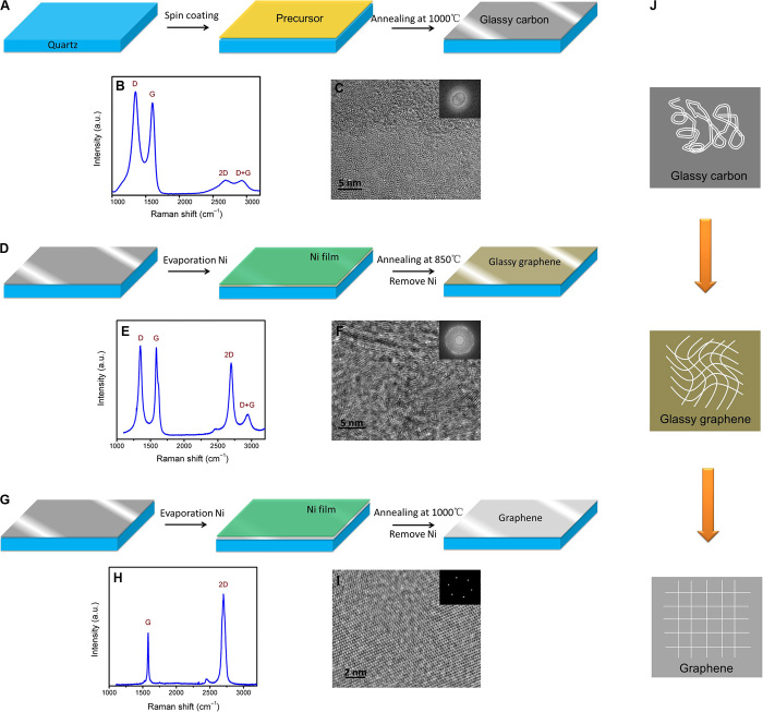
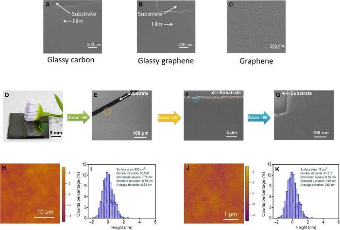
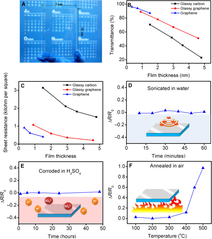
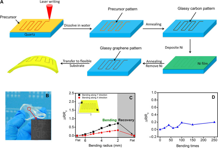
Large-area graphene thin films are prized in flexible and transparent devices. We report on a type of glassy graphene that is in an intermediate state between glassy carbon and graphene and that has high crystallinity but curly lattice planes. A polymer-assisted approach is introduced to grow an ultra-smooth (roughness, <0.7 nm) glassy graphene thin film at the inch scale. Owing to the advantages inherited by the glassy graphene thin film from graphene and glassy carbon, the glassy graphene thin film exhibits conductivity, transparency, and flexibility comparable to those of graphene, as well as glassy carbon-like mechanical and chemical stability. Moreover, glassy graphene-based circuits are fabricated using a laser direct writing approach. The circuits are transferred to flexible substrates and are shown to perform reliably. The glassy graphene thin film should stimulate the application of flexible transparent conductive materials in integrated circuits.

Keywords: Flexible; conducting; glassy graphene; graphene; laser direct writing; transparent; ultra-smooth.


Figures

Fig. 1
Fig. 1. Evolution from glassy carbon to glassy graphene and graphene.
(A to C) Synthesis process of a glassy carbon thin film and the corresponding Raman spectrum and HRTEM image. The inset to (C) shows the corresponding SAED pattern. (D to F) Synthesis of a glassy graphene thin film and the corresponding Raman spectrum and HRTEM image. The inset to (F) shows the corresponding SAED pattern. (G to I) Synthesis of a graphene thin film and the corresponding Raman spectrum and HRTEM image. The inset to (I) shows the corresponding SAED pattern. (J) Structure evolution from glassy carbon to glassy graphene and graphene.
Fig. 2
Fig. 2. Surface morphology of glassy graphene.
(A to C) SEM images of glassy carbon (A), glassy graphene (B), and graphene (C). (D) Optical image of a glassy graphene film on a quartz substrate with a daisy on top, showing the reflective surface of the glassy graphene film. (E) Microscopy image of the glassy graphene thin film; the scratch was made to provide contrast between the film and the substrate. (F and G) SEM image of the glassy graphene thin film. The colored dotted circles mark the zoom area respective to the zooming factors in the colored arrows. (H) AFM image (30 μm × 30 μm) of the glassy graphene film. (I) The distribution of heights of the AFM image (H). (J) AFM image (1 μm × 1 μm) of the glassy graphene film. (K) The distribution of heights of the AFM image (J).
Fig. 3
Fig. 3. Transmittance, conductivity, and robustness of glassy graphene.
(A) Image of the glassy graphene thin film on a quartz substrate (10 cm × 7 cm). (B) Transmittances of the glassy carbon, glassy graphene, and graphene with different thicknesses. (C) Sheet resistances of the glassy carbon, glassy graphene, and graphene with different thicknesses. (D) Mechanical toughness test of the glassy graphene film by sonication. (E) Chemical stability of the glassy graphene film under strong acid treatment [H2SO4 (pH 1)]. (F) Thermal stability of the glassy graphene film in air (annealed for 60 min at each point).
Fig. 4
Fig. 4. Preparation of glassy graphene–based circuits and the flexibility test.
(A) Laser direct writing of glassy graphene circuits. (B) Image of glassy graphene circuits on a flexible substrate. The inset shows the as-written circuits. (C) Variation in resistance of a glassy graphene film on a polydimethylsiloxane (PDMS) substrate at different bending radii. (D) The variation in resistance after repeated bending up to 250 times.

References

    1. Rogers J. A., Someya T., Huang Y., Materials and mechanics for stretchable electronics. Science 327, 1603–1607 (2010). - PubMed
    1. Sekitani T., Nakajima H., Maeda H., Fukushima T., Aida T., Hata K., Someya T., Stretchable active-matrix organic light-emitting diode display using printable elastic conductors. Nat. Mater. 8, 494–499 (2009). - PubMed
    1. Lipomi D. J., Vosgueritchian M., Tee B. C.-K., Hellstrom S. L., Lee J. A., Fox C. H., Bao Z., Skin-like pressure and strain sensors based on transparent elastic films of carbon nanotubes. Nat. Nanotechnol. 6, 788–792 (2011). - PubMed
    1. Xu F., Zhu Y., Highly conductive and stretchable silver nanowire conductors. Adv. Mater. 24, 5117–5122 (2012). - PubMed
    1. Pan S., Yang Z., Chen P., Deng J., Li H., Peng H., Wearable solar cells by stacking textile electrodes. Angew. Chem. Int. Ed. 53, 6110–6114 (2014). - PubMed

LinkOut - more resources