. 2017 Feb 21;114(8):1783-1788.
doi: 10.1073/pnas.1609839114. Epub 2017 Feb 7.

Pure circular polarization electroluminescence at room temperature with spin-polarized light-emitting diodes

Affiliations

Pure circular polarization electroluminescence at room temperature with spin-polarized light-emitting diodes

Nozomi Nishizawa et al. Proc Natl Acad Sci U S A. .

Abstract

We report the room-temperature electroluminescence (EL) with nearly pure circular polarization (CP) from GaAs-based spin-polarized light-emitting diodes (spin-LEDs). External magnetic fields are not used during device operation. There are two small schemes in the tested spin-LEDs: first, the stripe-laser-like structure that helps intensify the EL light at the cleaved side walls below the spin injector Fe slab, and second, the crystalline AlO x spin-tunnel barrier that ensures electrically stable device operation. The purity of CP is depressively low in the low current density (J) region, whereas it increases steeply and reaches close to the pure CP when J > 100 A/cm2 There, either right- or left-handed CP component is significantly suppressed depending on the direction of magnetization of the spin injector. Spin-dependent reabsorption, spin-induced birefringence, and optical spin-axis conversion are suggested to account for the observed experimental results.

Keywords: circular polarization; nonlinear effect; semiconductors; spin injection; spintronics.


Conflict of interest statement

The authors declare no conflict of interest.

Figures
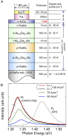
Fig. 1.
Fig. 1.
(A) A schematic cross section of spin-LEDs. (B) EL and PL spectra obtained from the control chip consisting of Au/Ti/γ-like AlOx/DHs. Solid lines represent EL spectra with three different current densities, J = 100 (σ+, red; and σ, black), 75 (green) and 50 (blue) A/cm2. The range of applied voltage is between 2–4 V. A black, dotted line shows PL spectrum obtained by the surface excitation ( = 1.58 eV, λ = 785 nm, 40 mW). The extinction coefficient of a top Au electrode is κ = 6.06 at 1.36 eV (λ = 909 nm) (39).
Fig. 2.
Fig. 2.
(A) A schematic experimental setup for EL measurements, showing, from upper left to lower right, a wire-bonded rectangle spin-LED chip on a copper block, a (λ/4) QWP, an LP, and an MCS. A pair of lenses, one between the chip and QWP and another between LP and MCS, is omitted for graphical clarity. Orange waves represent EL from the chip with right-handed (σ+, red circle) and left-handed (σ, blue circle) EL components. Straight orange arrows accompanied by double-headed arrows represent light waves converted into linear polarization by QWP. Thin dotted, blue arrows on polarizers represent optical axes. (Inset) Pictures of chip A with EL from the cleaved edge; current density J = 22 (Left) and 110 A/cm2 (Right). (B) A couple of helicity-specific EL spectra obtained when direction of remnant magnetization points toward QWP (+M, Upper) and against QWP (M, Lower).
Fig. 3.
Fig. 3.
JV curves of chip A in (A) linear scale and (B) semilogarithmic scale, together with (D) a plot CP value (PCP) against J. Somewhat larger bias voltage compared with the control sample suggests the formation of interface resistance in the Au/Ti/Fe/γ-AlOx electrode. (C) Helicity-specific EL spectra obtained at RT from a cleaved side wall of the chip at three different current densities: J = 22 (green), 55 (blue), and 110 (red) A/cm2, respectively. Solid and dotted lines show right-handed (σ+) and left-handed (σ) components, respectively. Three vertical arrows and dotted lines in A, B, and D represent the J values at which EL spectra are measured. The EL spectra measured at J = 110 A/cm2 are replotted in semilogarithmic scale in C (Inset).
Fig. S1.
Fig. S1.
Helicity-resolved EL spectra and circular polarization of chip A (Left), B (Middle), and C (Right) with the different current densities as specified in the figure.
Fig. 4.
Fig. 4.
Plots of (A) the integrated intensities of right-handed (σ+, closed symbols) and left-handed (σ, open symbols) components, (B) PCP values, (C) spectral width of the band B represented by full width at half maximum values, as a function of current density J for three different spin-LED chips, and horizontal line profiles of the PCP value and integrated EL intensity obtained from chip C at J = 75 (D) and 125 A/cm2 (E). The point y = 0 represents the position of a cleaved side right under the center of the Fe strip electrode (Inset). Measurements were carried out by laterally moving the 0.1-mm-wide, 10-mm-long, vertical optical slit that was placed 0.1 mm away from the cleaved edge.
Fig. S2.
Fig. S2.
Helicity-resolved EL spectra obtained at J = 39 A/cm2 for the chip without γ-AlOx tunnel barrier.
Fig. 5.
Fig. 5.
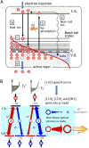
(A) A schematic illustration of transport–reabsorption scenario. The labels “Rad. rec.” and “Non-rad. rec.” represent radiative and nonradiative recombination processes, respectively. A red curve denotes the Fermi distribution function around the Fermi level (EF) that is shown by a dashed–dotted line. Hatched areas depict the states occupied by electrons (red) and holes (blue) above and below the Fermi level, respectively. Inside the area surrounded by a dotted line represents an active layer, whereas the outside denotes cladding layers (upper and lower spaces) and a free space (right and left spaces). (B) A schematic illustration that shows nonlinear effects in the optical process; electrical spin injection from an Fe spin injector into a 3D GaAs active layer through a 3D, n-AlGaAs clad layer (Upper), radiative recombination of [110], [11() 0] and [001] spins in conduction band (C.B.) with degenerated heavy- and light-holes in valence band (V.B.) (Lower Left), and conversion from elliptic polarization into pure CP through hypothetical nonlinear optical process (Lower Right).
Fig. S3.
Fig. S3.
Schematic illustration of transport–reabsorption scenario, incorporating time constants τj (j=14) associated with radiative recombination (process A), dielectric relaxation (process B), intraband relaxation (process C), and nonradiative recombination (process E), respectively, and photon lifetime of τph in a GaAs active layer.

References

    1. Hirohata A, Takanashi K. Future perspectives for spintronic devices. J Phys D Appl Phys. 2014;47(19):193001.
    1. Yuasa S, et al. Proc 2013 IEEE International Electron Devices Meeting (IEDM2013) Technical Digest. The Institute of Electrical and Electronics Engineers; Piscataway, New Jersey: 2013. Future Prospects of MRAM Technologies; pp. 3.1.1–3.1.4.
    1. Datta S, Das B. Electronic analog of the electro-optic modulator. Appl Phys Lett. 1990;56(7):665–667.
    1. Munekata H, et al. Diluted magnetic III-V semiconductors. Phys Rev Lett. 1989;63(17):1849–1852. - PubMed
    1. Wolf SA, et al. Spintronics: A spin-based electronics vision for the future. Science. 2001;294(5546):1488–1495. - PubMed

Publication types