. 2017 Mar 14:7:44576.
doi: 10.1038/srep44576.

Optimizing ultrathin Ag films for high performance oxide-metal-oxide flexible transparent electrodes through surface energy modulation and template-stripping procedures

Affiliations

Optimizing ultrathin Ag films for high performance oxide-metal-oxide flexible transparent electrodes through surface energy modulation and template-stripping procedures

Xi Yang et al. Sci Rep. .

Abstract

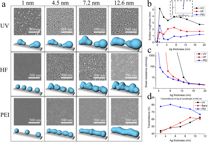
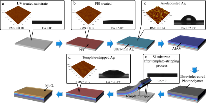
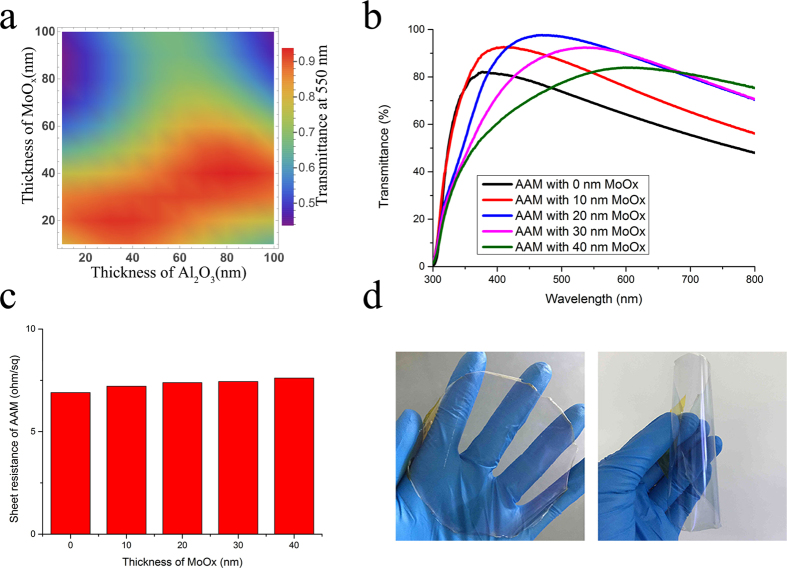
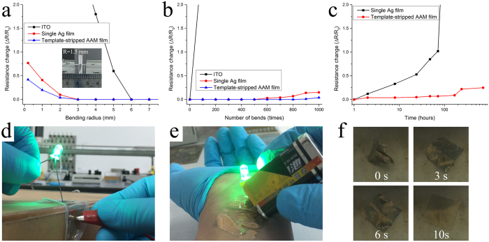
Among new flexible transparent conductive electrode (TCE) candidates, ultrathin Ag film (UTAF) is attractive for its extremely low resistance and relatively high transparency. However, the performances of UTAF based TCEs critically depend on the threshold thickness for growth of continuous Ag films and the film morphologies. Here, we demonstrate that these two parameters could be strongly altered through the modulation of substrate surface energy. By minimizing the surface energy difference between the Ag film and substrate, a 9 nm UTAF with a sheet resistance down to 6.9 Ω sq-1 can be obtained using an electron-beam evaporation process. The resultant UTAF is completely continuous and exhibits smoother morphologies and smaller optical absorbances in comparison to the counterpart of granular-type Ag film at the same thickness without surface modulation. Template-stripping procedure is further developed to transfer the UTAFs to flexible polymer matrixes and construct Al2O3/Ag/MoOx (AAM) electrodes with excellent surface morphology as well as optical and electronic characteristics, including a root-mean-square roughness below 0.21 nm, a transparency up to 93.85% at 550 nm and a sheet resistance as low as 7.39 Ω sq-1. These AAM based electrodes also show superiority in mechanical robustness, thermal oxidation stability and shape memory property.


Conflict of interest statement

The authors declare no competing financial interests.

Figures

Figure 1
Figure 1. Performance of Ag films.
(a) Scanning electron microscopy images showing morphological differences between 1-, 4.5-, 7.2- and 12.6-nm-thick Ag films deposited on silicon substrates with pre-treatments by UV, HF and PEI, respectively. Scale bar, 500 nm. Conceptual diagrams showing the cluster coalescence mechanism of Ag film on each stage. (b) Root-mean-square surface roughness of Ag films on different substrates varying with Ag thickness. Average surface roughness was determined from the measurement of at least three different scan domains for each sample. The inset shows the RMS of three substrates. (c) Variations in sheet resistance of Ag films on different silicon substrates as a function of Ag thickness. (d) Transmittance of Ag film on UV treated, bare, and PEI treated quartz substrates, respectively, at the wavelength of 450 nm.
Figure 2
Figure 2. Schematic illustration of the process for fabricating the AAM based TEs.
AFM images and photographs of the measured contact angle of (a) UV treated substrate, (b) PEI treated substrate, (c) As-deposited Ag film and (d) Template-stripped Ag film. (e) Si substrate after the template-stripping process, the CA indicate that the PEI was peeled off together with Ag film after the template-stripping process.
Figure 3
Figure 3. Performance of AAM based TEs.
(a) Calculated transmittance of AAM film at the wavelength of 550 nm as a function of the thickness of MoOx and Al2O3 layers. The thickness of Ag is fixed at 9 nm. (b) Transmittance spectra and (c) sheet resistance of AAM film with a fixed Al2O3 thickness at 9 nm and various MoOx thicknesses in experiment. (d) Optical photographs of flexible AAM based TCEs peeled off from 4-in wafer size silicon by template-stripping process.
Figure 4
Figure 4. Flexibility and stability of AAM based TEs.
(a) Relative change in the resistances of the ITO on PET, single Ag layer on PET, and stripped AAM film as a function of bending radius. The inset shows a photograph of a folded AAM based TCE with a bending radius of 1.5 mm set for the bending test. (b) Relative changes in the resistances of the ITO, single Ag, and stripped AAM film as a function of the number of bending cycles at the bending radius of 3 mm. (c) Relative changes in the resistance of the single Ag and stripped AAM film as a function of the exposing time up to 1000 hours. Photographs of blue LED lamps mounted on flexible AAM based TCE on (d) sharp wooded edge and (e) human skin. (f) A series of photographs showing the shape memory property of flexible AAM based TCE after baked at 100 °C.

References

    1. Lee S. et al. A transparent bending-insensitive pressure sensor. Nat. Nanotechnol. 11, 472–478 (2016). - PubMed
    1. Kim C.-C., Lee H.-H., Oh K. H. & Sun J.-Y. Highly stretchable, transparent ionic touch panel. Science 353, 682–687 (2016). - PubMed
    1. Jiang X.-Z., Sun Y.-J., Fan Z. & Zhang T.-Y. Integrated Flexible, Waterproof, Transparent, and Self-Powered Tactile Sensing Panel. Acs Nano 10, 7696–7704 (2016). - PubMed
    1. Gao W. et al. Fully integrated wearable sensor arrays for multiplexed in situ perspiration analysis. Nature 529, 509–514 (2016). - PMC - PubMed
    1. Lee W. et al. Organic-acid texturing of transparent electrodes toward broadband light trapping in thin-film solar cells. Nano Energy 17, 180–186 (2015).

Publication types