

Effects of GaN/AlGaN/Sputtered AlN nucleation layers on performance of GaN-based ultraviolet light-emitting diodes
- PMID: 28294166
- PMCID: PMC5353678
- DOI: 10.1038/srep44627
Effects of GaN/AlGaN/Sputtered AlN nucleation layers on performance of GaN-based ultraviolet light-emitting diodes
Abstract
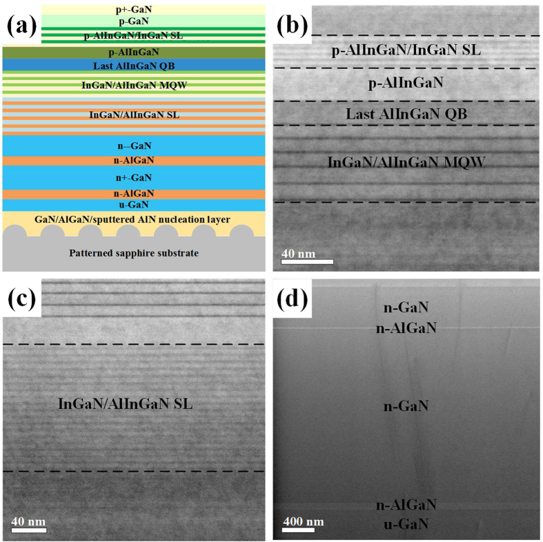
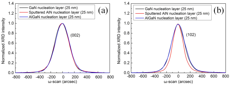
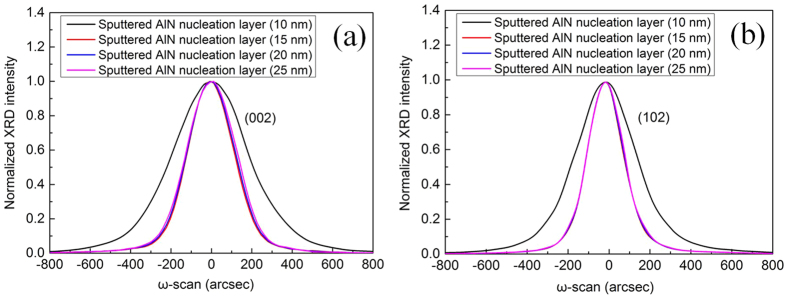
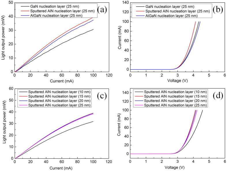
We report on the demonstration of GaN-based ultraviolet light-emitting diodes (UV LEDs) emitting at 375 nm grown on patterned sapphire substrate (PSS) with in-situ low temperature GaN/AlGaN nucleation layers (NLs) and ex-situ sputtered AlN NL. The threading dislocation (TD) densities in GaN-based UV LEDs with GaN/AlGaN/sputtered AlN NLs were determined by high-resolution X-ray diffraction (XRD) and cross-sectional transmission electron microscopy (TEM), which revealed that the TD density in UV LED with AlGaN NL was the highest, whereas that in UV LED with sputtered AlN NL was the lowest. The light output power (LOP) of UV LED with AlGaN NL was 18.2% higher than that of UV LED with GaN NL owing to a decrease in the absorption of 375 nm UV light in the AlGaN NL with a larger bandgap. Using a sputtered AlN NL instead of the AlGaN NL, the LOP of UV LED was further enhanced by 11.3%, which is attributed to reduced TD density in InGaN/AlInGaN active region. In the sputtered AlN thickness range of 10-25 nm, the LOP of UV LED with 15-nm-thick sputtered AlN NL was the highest, revealing that optimum thickness of the sputtered AlN NL is around 15 nm.
Conflict of interest statement
The authors declare no competing financial interests.
Figures
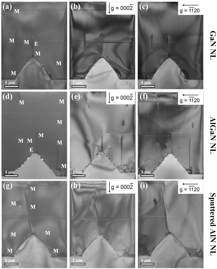
 ]. Bright-filed TEM images of UV LED with (b) GaN NL, (e) AlGaN NL, and (h) sputtered AlN NL when g = 0002. Bright-filed TEM images of UV LED with (c) GaN NL, (f) AlGaN NL, and (i) sputtered AlN NL when g =
  .
.
References
-
- Khan A., Balakrishnan K. & Katona T. Ultraviolet light-emitting diodes based on group three nitrides. Nat. photon 2, 77–84 (2008).
-
- Kneissl M. et al. Advances in group III-nitride-based deep UV light-emitting diode technology. Semicond. Sci. Technol. 26, 014036 (2011).
-
- Hirayama H. et al. 222–282 nm AlGaN and InAlGaN-based deep-UV LEDs fabricated on high-quality AlN on sapphire. Phys. Status Solidi A. 206, 1176–1182 (2009).
-
- Dai Q. L., Foley M. E., Breshike C. J., Lita A. & Strouse G. F. Ligand-Passivated Eu:Y2O3 Nanocrystals as a Phosphor for White Light Emitting Diodes. J. Am. Chem. Soc. 133, 15475–15486 (2011). - PubMed
Publication types
LinkOut - more resources
Full Text Sources
Other Literature Sources
