. 2017 Mar 15:7:44361.
doi: 10.1038/srep44361.

Anisotropic electrical resistance in mesoscopic LaAlO3/SrTiO3 devices with individual domain walls

Affiliations

Anisotropic electrical resistance in mesoscopic LaAlO3/SrTiO3 devices with individual domain walls

Nicholas J Goble et al. Sci Rep. .

Abstract

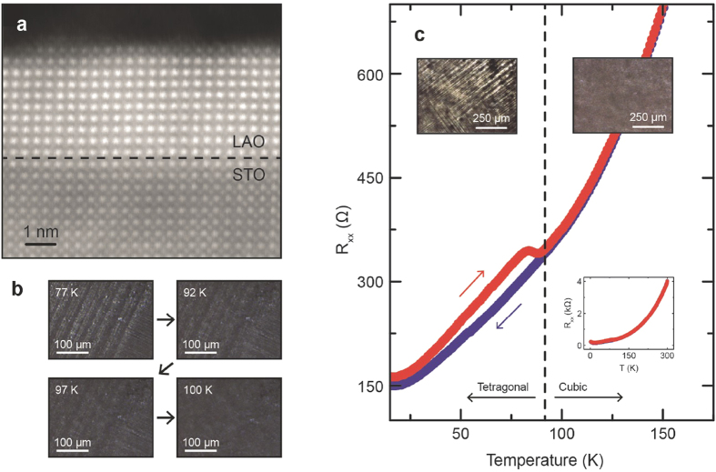
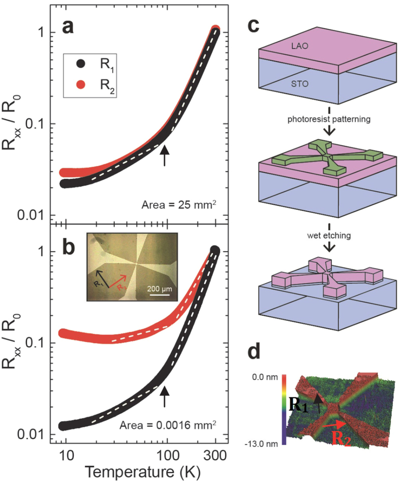
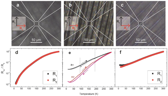
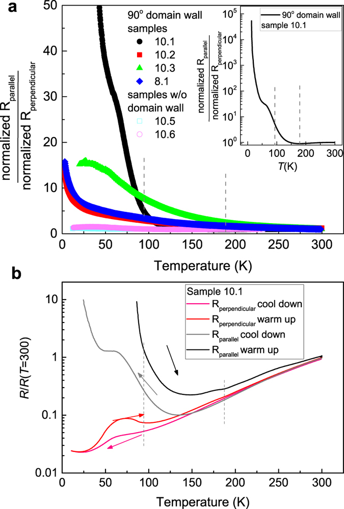
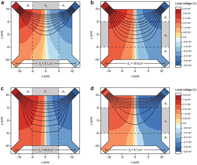
The crystal structure of bulk SrTiO3(STO) transitions from cubic to tetragonal at around 105 K. Recent local scanning probe measurements of LaAlO3/SrTiO3 (LAO/STO) interfaces indicated the existence of spatially inhomogeneous electrical current paths and electrostatic potential associated with the structural domain formation in the tetragonal phase of STO. Here we report a study of temperature dependent electronic transport in combination with the polarized light microscopy of structural domains in mesoscopic LAO/STO devices. By reducing the size of the conductive interface to be comparable to that of a single tetragonal domain of STO, the anisotropy of interfacial electron conduction in relationship to the domain wall and its direction was characterized between T = 10-300 K. It was found that the four-point resistance measured with current parallel to the domain wall is larger than the resistance measured perpendicular to the domain wall. This observation is qualitatively consistent with the current diverting effect from a more conductive domain wall within the sample. Among all the samples studied, the maximum resistance ratio found is at least 10 and could be as large as 105 at T = 10 K. This electronic anisotropy may have implications on other oxide hetero-interfaces and the further understanding of electronic/magnetic phenomena found in LAO/STO.


Conflict of interest statement

The authors declare no competing financial interests.

Figures

Figure 1
Figure 1. Cubic-to-tetragonal phase transition in LAO/STO and its effect on electron transport in large samples.
(a) HAADF-STEM (High-Angle Annular Dark-Field Scanning Transmission Electron Microscopy) image of LAO/STO interface. Imaged sample has 10 unit cells of LAO and was grown by PLD in 10−4 Torr O2 partial pressure. (b) Polarized transmission microscopy images of LAO/STO showing tetragonal domains at different temperatures. Tetragonal domain walls disappear between 97 K and 100 K. (c) Temperature dependent resistance R(T) of a 5 mm × 5 mm large 10 u.c. LAO/STO sample. Arrows indicate temperature sweep direction, showing hysteresis below ~90 K. Insets show temperature dependent resistance from 2 K–300 K and polarized microscopy images of an area in the sample in the tetragonal and cubic phases.
Figure 2
Figure 2. Temperature dependent resistance for a 10 u.c.
LAO/STO sample before (a) and after (b) patterning. R1 and R2 indicate resistances taken with current and voltage contact configuration rotated by 90° (see inset of (b) and (d)). Inset is a standard microscopy image of the etched van der Pauw pattern. The black arrow and white dashed lines in (a) and (b) are a guide to the eye to show the position of the cubic-tetragonal transition and the slope change in R(T). The process of etching the sample is shown in (c). A photoresist mask is patterned on bare LAO/STO, which is subsequently etched. The mask is removed, leaving only the conductive interface covered by the pattern. After the process is complete, the sample topography was imaged using an optical profilometer (d).
Figure 3
Figure 3. Resistance anisotropy in mesoscopic samples with domain wall in the tetragonal phase of STO.
(a,b,c) Overlays of domain images and the conductive van der Pauw patterns (outlined in white). Images and data show samples at 77 K with no domain walls (a), an extra striped domain at ~80° (b), and an extra domain at ~45°(c) to the sample edge, respectively. Images (d,e,f) show the temperature dependent longitudinal resistance (normalized over the 300 K value) for two measurement orientations marked in (ac). Resistance is isotropic with no domain wall (a) and 45° wall (c) and is anisotropic with 80° domain wall (b). All samples are 10 u.c. thick and grown at 10−4 Torr O2 pressure (samples in (ac) correspond to sample no. 10.6, 10.3 and 10.4 in the Table S1 of SI).
Figure 4
Figure 4
(a) Anisotropy strength in various LAO/STO samples split by one or two domain walls at ~90° vs. those without domain walls. All samples had 8–10 u.c. thick LAO and were grown at 10−4 or 10−5 Torr O2 pressure. Samples with a ~90° domain wall show an anisotropy ratio between 10 and 100000 at T = 10 K. The inset shows the anisotropy ratio in log-scale for sample 10.1 which had the largest anisotropy. The two vertical dashed lines mark the temperatures for the two structural phase transitions. (b) The cool-down vs. warm-up R(T) curves for sample 10.1 along the two measurement directions, showing the hysteresis effects.
Figure 5
Figure 5. Simulated current flow and voltage distribution for inhomogeneous 20 μm × 20 μm Van der Pauw patterns.
The conductive squares are split by 10 μm wide regions with different resistivity, where ρ1=25,000 Ω and ρ2 = 10,000 Ω. Total current flow is 10 nA in all simulations and is represented with streamlines. Simulated samples in (a) and (b) are split by more conductive regions oriented perpendicular and parallel to the current flow, respectively. When a conductive region splits the sample, measured Vparallel, and therefore Rparallel (b) is greater than Vperpendicular and Rperpendicular (a), due to the more conducting center stripe diverting current towards voltage contacts. However, when the samples are split by a more resistive area as in (c) and (d), the sample shows smaller voltage probed by the voltage contacts in the parallel configuration (d) due to the more resistive center stripe suppressing the current flowing between voltage contacts.

Similar articles

Cited by

References

    1. Cowley R. A. Lattice Dynamics and Phase Transitions of Strontium Titanate. Phys. Rev. 134, A981 (1964).
    1. Lytle F. W. X-Ray Diffractometry of Low-Temperature Phase Transformations in Strontium Titanate. J. Appl. Phys. 35, 2212 (1964).
    1. Ohtomo A. & Hwang H. Y. A high-mobility electron gas at the LaAlO3/SrTiO3 heterointerface. Nature 427, 423–426 (2004). - PubMed
    1. Nakagawa N., Hwang H. Y. & Muller D. A. Why some interfaces cannot be sharp. Nature Materials 5, 204–209 (2006).
    1. Mannhart J., Blank D. H. A., Hwang H. Y., Millis A. J. & Triscone J. M. Two-dimensional electron gases at oxide interfaces. MRS Bulletin, 33, 1027–1034 (2008).

Publication types

LinkOut - more resources