. 2017 Mar 15;7(1):184.
doi: 10.1038/s41598-017-00251-3.

Considerable knock-on displacement of metal atoms under a low energy electron beam

Affiliations

Considerable knock-on displacement of metal atoms under a low energy electron beam

Hengfei Gu et al. Sci Rep. .

Abstract

Under electron beam irradiation, knock-on atomic displacement is commonly thought to occur only when the incident electron energy is above the incident-energy threshold of the material in question. However, we report that when exposed to intense electrons at room temperature at a low incident energy of 30 keV, which is far below the theoretically predicted incident-energy threshold of zirconium, Zircaloy-4 (Zr-1.50Sn-0.25Fe-0.15Cr (wt.%)) surfaces can undergo considerable displacement damage. We demonstrate that electron beam irradiation of the bulk Zircaloy-4 surface resulted in a striking radiation effect that nanoscale precipitates within the surface layer gradually emerged and became clearly visible with increasing the irradiation time. Our transmission electron microscope (TEM) observations further reveal that electron beam irradiation of the thin-film Zircaly-4 surface caused the sputtering of surface α-Zr atoms, the nanoscale atomic restructuring in the α-Zr matrix, and the amorphization of precipitates. These results are the first direct evidences suggesting that displacement of metal atoms can be induced by a low incident electron energy below threshold. The presented way to irradiate may be extended to other materials aiming at producing appealing properties for applications in fields of nanotechnology, surface technology, and others.


Conflict of interest statement

The authors declare that they have no competing interests.

Figures

Figure 1
Figure 1
Surface morphology evolutions of pure Zr and Zircaloy-4 specimens under irradiation at room temperature with focused and stationary electron beam at an incident energy of 30 keV in the FE-SEM. (a–e) SEM images of the selected surface area of the polished bulk pure zirconium specimen after irradiation for 1, 8, 16, 24, and 32 electron beam scans, respectively. (fj) SEM images of the selected surface area of the polished bulk Zircaloy-4 specimen after irradiation for 1, 8, 16, 24, and 32 electron beam scans, respectively. The clearly visible ball-shaped zirconia particles (red arrows in Fig. 1a and f) suspended on the surface indicate that the SEM images were taken when the surface was clearly focused. (ko) SEM images of the selected thin film region in the vicinity of the hole of the Zircaloy-4 TEM specimen after irradiation for 1, 32, 64, 96, and 128 electron beam scans, respectively. The area outlined by a blue square in every image is expanded in its corresponding inset outlined by a red square, which shows the morphology of the precipitate of interest (yellow arrow in the inset). (p,q) SEM and TEM images showing that the electron beam irradiation in the FE-SEM and the microstructure observation in the TEM were performed on the same thin film region of the Zircaloy-4 TEM specimen containing the precipitate of interest (yellow arrows in Fig. 1p and q).
Figure 2
Figure 2
Compositional analysis. (a) The expanded surface morphology of the area outlined by a red square in Fig. 1j. (bc) EDS spectra and compositions corresponding to Point 1 and 2 in Fig. 2a, respectively. (d–h) STEM image showing morphologies of precipitates (ball-shaped nanoparticles with dark contrast) in Zircaloy-4 (d) and its corresponding Zr L (e), Sn L (f), Fe K (g), and Cr K (h) elemental maps.
Figure 3
Figure 3
TEM observations of the precipitate of interest and its surrounding α-Zr matrix before and after irradiation at room temperature with focused and stationary electron beam at an incident energy of 30 keV in the FE-SEM viewed along the [112¯3]α-Zr direction. Column A–E of Fig. 3 shows TEM results before and after irradiation for 32, 64, 96, and 128 electron beam scans, respectively. Row a of Fig. 3 shows BF TEM images of the precipitate of interest and its surrounding α-Zr matrix. Row b of Fig. 3 shows composite SAED patterns of the precipitate of interest and its surrounding α-Zr matrix. Row c–e of Fig. 3 show HRTEM images and their corresponding FFT diffraction patterns corresponding to the center (not the same position), the up-left corner (Area 1 in Fig. 3(A-a-1)) and the down-right corner (Area 2 in Fig. 3(A-a-1)) of the precipitate of interest, respectively. In Row c of Fig. 3, the FFT diffraction pattern in every column corresponds to the area outlined by a yellow square in the corresponding HRTEM image. In Row d and e of Fig. 3, the left and right FFT diffraction patterns in every column of Fig. 3 correspond to the areas outlined by blue and green squares in the corresponding HRTEM image, respectively.
Figure 4
Figure 4
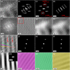
Moiré fringes at the perimeter of the precipitate of interest. (a) HRTEM image showing an area where fringes disappeared at the interior of the precipitate viewed along the [112¯3]α-Zr direction. (e) The FFT diffraction pattern corresponding to Fig. 4a. (b,c and d) The partially masked FFT diffraction patterns corresponding to Fig. 4c. (f,g and h) The noise-filtered IFFT images corresponding to Fig. 4a obtained by using the partially masked FFT diffraction patterns in Fig. 4(b,c and d), respectively. In Fig. e, b and c, it can be seen that every FFT diffraction spot (including the central FFT diffraction spot) belonging to α-Zr phase along [112¯3]α-Zr diverges into three spots. (i) The expanded morphology of the area outlined by a red square in Fig. 4f. (j,k and l) The three diverged FFT diffraction spots corresponding to the (101¯1¯)α-Zr planes, respectively. (o,p and q) The IFFT images corresponding to Fig. 4i obtained by using the masked FFT diffraction spots in Fig. 4j, k and l, respectively. (m) The three diverged spots of the central FFT diffraction spot. (n) The IFFT image corresponding to Fig. 4i obtained by using the masked FFT diffraction spots in Fig. 4m. The divergence of the FFT diffraction pattern corresponding to α-Zr phase along [112¯3]α-Zr as well as the central FFT diffraction spot is due to the presence of the fringes. Take the (101¯1¯)α-Zr planes for example. The (101¯1¯)α-Zr planes on fringes (pink bar in Fig. 4i) can still form periodic planes (Fig. 4o). The (101¯1¯)α-Zr planes on Fringe 1 in Fig. 4i can line up with their two adjacent (101¯1¯)α-Zr planes on Fringe 2 in Fig. 4i (green and yellow bars in Fig. 4i) and form periodic planes (Fig. 4p and q), respectively. In addition, the fringes themselves are periodic, resulting in the divergence of the central FFT diffraction spot as seen in Fig. 4n and m.
Figure 5
Figure 5
Changes of atomic structure within the α-Zr matrix after irradiation at room temperature with focused and stationary electron beam at an incident energy of 30 keV in the FE-SEM viewed along the [112¯3]α-Zr direction. (a) and (k) HRTEM images of two typical areas of the α-Zr matrix containing electron-beam-induced changes of atomic structure. (f) and (n) The FFT diffraction patterns corresponding to Fig. 5a and k, respectively. (b,c,d and e) The partially masked FFT diffraction patterns corresponding to Fig. 5f. (g,h,i and j) The noise-filtered IFFT images corresponding to Fig. 5a obtained by using the partially masked FFT diffraction patterns in Fig. 5b,c,d and e, respectively. The insets in Fig. 5g,h,i and j show the expanded morphologies of the areas outlined by blue squares in Fig. 5g,h,i and j, respectively. (l) and (m) The partially masked FFT diffraction patterns corresponding to Fig. 5n. (o) and (p) The noise-filtered IFFT images corresponding to Fig. 5k obtained by using the partially masked FFT diffraction patterns in Fig. 5l and m, respectively. The insets in Fig. 5o and p show the expanded morphologies of the areas outlined by blue squares in Fig. 5o and p, respectively. The yellow ‘T's in Fig. 5p indicate the electron-beam-induced dislocations.

Similar articles

Cited by

References

    1. Was, G. S. Fundamentals of radiation materials science: metals and alloys (Springer, New York, 2007).
    1. Murty, K. L., Charit, I. An introduction to nuclear materials: fundamentals and applications (Wiley-VCH, Weinheim, 2013).
    1. Hren, J. J., Goldstein, J. I. & Joy, D. C. Introduction to analytical electron microscopy (Springer, New York, 1979).
    1. Williams, D. B. & Carter C. B. Transmission electron microscopy: a textbook for materials science (Springer, New York, 2009).
    1. Egerton RF, Li P, Malac M. Radiation damage in the TEM and SEM. Micron. 2004;35:399–409. doi: 10.1016/j.micron.2004.02.003. - DOI - PubMed

LinkOut - more resources