. 2017 Jan 13;7(1):17.
doi: 10.3390/nano7010017.

Nano-Photonic Structures for Light Trapping in Ultra-Thin Crystalline Silicon Solar Cells

Affiliations

Nano-Photonic Structures for Light Trapping in Ultra-Thin Crystalline Silicon Solar Cells

Prathap Pathi et al. Nanomaterials (Basel). .

Abstract

Thick wafer-silicon is the dominant solar cell technology. It is of great interest to develop ultra-thin solar cells that can reduce materials usage, but still achieve acceptable performance and high solar absorption. Accordingly, we developed a highly absorbing ultra-thin crystalline Si based solar cell architecture using periodically patterned front and rear dielectric nanocone arrays which provide enhanced light trapping. The rear nanocones are embedded in a silver back reflector. In contrast to previous approaches, we utilize dielectric photonic crystals with a completely flat silicon absorber layer, providing expected high electronic quality and low carrier recombination. This architecture creates a dense mesh of wave-guided modes at near-infrared wavelengths in the absorber layer, generating enhanced absorption. For thin silicon (<2 μm) and 750 nm pitch arrays, scattering matrix simulations predict enhancements exceeding 90%. Absorption approaches the Lambertian limit at small thicknesses (<10 μm) and is slightly lower (by ~5%) at wafer-scale thicknesses. Parasitic losses are ~25% for ultra-thin (2 μm) silicon and just 1%-2% for thicker (>100 μm) cells. There is potential for 20 μm thick cells to provide 30 mA/cm² photo-current and >20% efficiency. This architecture has great promise for ultra-thin silicon solar panels with reduced material utilization and enhanced light-trapping.

Keywords: light-trapping; nano-photonics; scattering; solar cell.


Conflict of interest statement

The authors declare no conflict of interest. The founding sponsors had no role in the design of the study; in the collection, analyses, or interpretation of data; in the writing of the manuscript, and in the decision to publish the results.

Figures
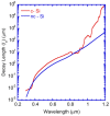
Figure 1
Figure 1
Photon absorption length as a function of wavelength for crystalline silicon (c-Si) and nano- crystalline silicon (nc-Si) (using the complex refractive index (n, k) parameters of Reference [26]).
Figure 2
Figure 2
Proposed solar architecture consists of thin flat spacer titanium dioxide (TiO2) layers on the front and rear surfaces of silicon, nanocone gratings on both sides with optimized pitch and height, and rear cones are surrounded by Ag metal reflector.
Figure 3
Figure 3
(a) Cell structure used for optimization of texture parameter using simulations. The structure consists of thin flat TiO2 layers on the front and rear surfaces of flat silicon (1 μm). The cones are only on the front surface without rear cones and Ag metal reflector; (b) Weighted absorption, <Aw> and (c) Short-circuit current density, JSC, as a function of cone height for different pitch values. Figure shows optimum pitch >750 nm and cone height >500 nm with an increasing trend of tolerance of optimum cone height at larger pitch.
Figure 4
Figure 4
Sequence of light trapping structures on flat silicon. (a) Grating-free cell with thin layers of 60 and 50 nm on front and rear surface, respectively, and flat Ag back-reflector; (b) Front-grating cell with only front cones of height of 600 nm and a pitch of 750 nm and flat Ag back-reflector; (c) Rear-grating cell with only rear cones of height of 200 nm and a pitch of 750 nm and corrugated Ag back-reflector; (d) Dual-grating cell with a combination of front and rear cones with optimized parameters used in ‘b’ and ‘c’ with corrugated Ag back-reflector.
Figure 5
Figure 5
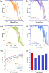
Comparison of absorption spectra of planar silicon with 4n2 absorption limit for different light trapping configurations shown in Figure 2 such as (a) grating-free cell, (b) front-grating cell, (c) rear-grating cell, and (d) dual-grating cell using the optimized grating parameter for 2 μm silicon; (e) Comparison of JSC of planar cell for different light trapping configurations shown in Figure 2 with respect to silicon thickness using optimized grating parameters for 2 μm silicon; (f) JSC of the cell for a particular thickness of 2 μm for four different configurations.
Figure 6
Figure 6
(a) Absorption spectra of the dual-grating cell (c-Si thickness = 2 μm) and (b) corresponding JSC of the cell as a function of angle of incidence (AoI) in the range 0°–85° in steps of 5° (inset shows the JSC of grating-free cell for p- and s-polarization and its average). The average absorption is more than 80% over a wide wavelength band. JSC is independent of polarization and is less influenced until the AoI reaches 70°, showing the omni-directionality of the nanocone grating structures.
Figure 7
Figure 7
Electric field intensity distribution across the silicon absorber layer at an incident wavelength of (a) 500 nm and (b) 700 nm for the dual-grating cell with optimized parameters for the front and rear nano-cone arrays. The incident electric field intensity is normalized to 1.
Figure 8
Figure 8
Comparison of the simulated short-circuit photo-current JSC as a function of the thickness of the Si absorber layer in the real-space method utilizing only the absorption in the Si layer, compared to the Fourier space method which includes the absorption in all layers. The difference between the real-space and Fourier space results is the parasitic absorption. The Lambertian limit is shown for comparison.
Figure 9
Figure 9
Schematic of the TiO2 nanoimprinting process. (1) TiO2 film is spin-coated on silicon substrate using a precursor titanium diisopropoxide bis(acetylacetonate); (2) The polydimethylsiloxane (PDMS) stamp having nanocups is placed on the spin-coated film with patterned side facing the film. The whole assembly is sandwiched between two glass slides and held together with binder clips (not shown here); (3) After keeping at ~170 °C for 15 min, the binder clips are released to reveal the inverse of PDMS nanocups on the TiO2 film.
Figure 10
Figure 10
(a) Atomic force microscopy (AFM) image of the periodic array of nanocones imprinted on TiO2 film. The AFM line scan shows the periodicity at ~750 nm and the average height of nanocones at ~35 nm; (b) Three-dimensional view of the structure showing titania nanocone arrays.

References

    1. National Renewable Energy Laboratory (NREL) National Center for Photovoltaics Solar Efficiency Chart. [(accessed on 30 December 2016)]; Available online: http://www.nrel.gov/pv/assets/images/efficiency_chart.jpg.
    1. Green M.A., Emery K., Hishikawa Y., Warta W., Dunlop E.D. Solar Efficiency Tables (version 47) Prog. Photovolt. 2016;24:3–11. doi: 10.1002/pip.2728. - DOI
    1. Atwater H., Polman A. Plasmonics for improved photonic devices. Nat. Photonics. 2010;9:9–16. - PubMed
    1. Palik E. Handbook of the Optical constants of Solids. Academic Press; San Diego, CA, USA: 1998.
    1. Biswas R., Xu C. Nano-crystalline silicon solar cell architecture with absorption at the classical 4n2 limit. Opt. Exp. 2011;19:A672. doi: 10.1364/OE.19.00A664. - DOI - PubMed

LinkOut - more resources